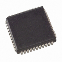
AT49LV1025-70JC Atmel, AT49LV1025-70JC Datasheet - Page 3

AT49LV1025-70JC
Manufacturer Part Number
AT49LV1025-70JC
Description
IC FLASH 1MBIT 70NS 44PLCC
Manufacturer
Atmel
Datasheet
1.AT49LV1024.pdf
(15 pages)
Specifications of AT49LV1025-70JC
Format - Memory
FLASH
Memory Type
FLASH
Memory Size
1M (64K x 16)
Speed
70ns
Interface
Parallel
Voltage - Supply
3 V ~ 3.6 V
Operating Temperature
0°C ~ 70°C
Package / Case
44-PLCC
Lead Free Status / RoHS Status
Contains lead / RoHS non-compliant
AT49LV1024/1025
The program cycle has addresses latched on the falling edge of WE or CE, whichever
occurs last, and the data latched on the rising edge of WE or CE, whichever occurs first.
Programming is completed after the specified t
cycle time. The Data Polling feature
BP
may also be used to indicate the end of a program cycle.
BOOT BLOCK PROGRAMMING LOCKOUT: The device has one designated block
that has a programming lockout feature. This feature prevents programming of data in
the designated block once the feature has been enabled. The size of the block is 8K
words. This block, referred to as the boot block, can contain secure code that is used to
bring up the system. Enabling the lockout feature will allow the boot code to stay in the
device while data in the rest of the device is updated. This feature does not have to be
activated; the boot block’s usage as a write-protected region is optional to the user. The
address range of the boot block is 0000H to 1FFFH.
Once the feature is enabled, the data in the boot block can no longer be erased or pro-
grammed. Data in the main memory block can still be changed through the regular
programming method and can be erased using either the Chip Erase or the Main Mem-
ory Block Erase command. To activate the lockout feature, a series of six program
commands to specific addresses with specific data must be performed. Please refer to
the Command Definitions table.
BOOT BLOCK LOCKOUT DETECTION: A software method is available to determine if
programming of the boot block section is locked out. When the device is in the software
product identification mode (see Software Product Identification Entry and Exit sections)
a read from address location 0002H will show if programming the boot block is locked
out. If the data on I/O0 is low, the boot block can be programmed; if the data on I/O0 is
high, the program lockout feature has been activated and the block cannot be pro-
grammed. The software product identification exit code should be used to return to
standard operation.
PRODUCT IDENTIFICATION: The product identification mode identifies the device and
manufacturer as Atmel. It may be accessed by hardware or software operation. The
hardware operation mode can be used by an external programmer to identify the correct
programming algorithm for the Atmel product.
For details, see “Operating Modes” (for hardware operation) or “Software Product Identi-
fication Entry/Exit” on page 11. The manufacturer and device code is the same for both
modes.
DATA POLLING: The AT49LV1024/1025 features Data Polling to indicate the end of a
program or erase cycle. During a program cycle an attempted read of the last byte
loaded will result in the complement of the loaded data on I/O7. Once the program cycle
has been completed, true data is valid on all outputs and the next cycle may begin. Data
Polling may begin at any time during the program cycle.
TOGGLE BIT: In addition to Data Polling, the AT49LV1024/1025 provides another
method for determining the end of a program or erase cycle. During a program or erase
operation, successive attempts to read data from the device will result in I/O6 toggling
between one and zero. Once the program cycle has completed, I/O6 will stop toggling
and valid data will be read. Examining the toggle bit may begin at any time during a pro-
gram cycle.
HARDWARE DATA PROTECTION: Hardware features protect against inadvertent
writes to the AT49LV1024/1025 in the following ways: (a) V
sense: if V
is below
CC
CC
1.8V (typical), the program function is inhibited. (b) Program inhibit: holding any one of
OE low, CE high or WE high inhibits program cycles. (c) Noise filter: pulses of less than
15 ns (typical) on the WE or CE inputs will not initiate a program cycle.
3
1278D–07/01


