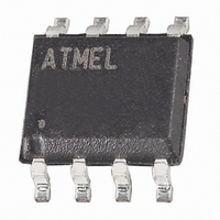
AT93C86A-10SI-2.7 Atmel, AT93C86A-10SI-2.7 Datasheet

AT93C86A-10SI-2.7
Specifications of AT93C86A-10SI-2.7
Available stocks
Related parts for AT93C86A-10SI-2.7
AT93C86A-10SI-2.7 Summary of contents
Page 1
... The CC device is optimized for use in many industrial and commercial applications where low- power and low-voltage operations are essential. The AT93C86A is available in space saving 8-lead PDIP, 8-lead JEDEC SOIC, 8-lead Ultra Thin lead TSSOP packages. ...
Page 2
... Meg ohm pullup, then the x 16 organization is selected. AT93C86A 2 The AT93C86A is enabled through the Chip Select pin (CS), and accessed via a three- wire serial interface consisting of Data Input (DI), Data Output (DO), and Shift Clock (SK). Upon receiving a Read instruction at DI, the address is decoded and the data is clocked out serially on the data output pin DO ...
Page 3
Table 2. Pin Capacitance Applicable over recommended operating range from T Symbol Test Conditions C Output Capacitance (DO) OUT C Input Capacitance (CS, SK, DI) IN Note: 1. This parameter is characterized and is not 100% tested. Table 3. ...
Page 4
... Output Delay to “0” PD0 Status Valid High t DF Impedance t Write Cycle Time WP (1) Endurance 5.0V, 25°C Note: 1. This parameter is ensured by characterization. AT93C86A 4 = −40° 85° Test Condition 4.5V ≤ V ≤ 5.5V CC 2.7V ≤ V ≤ 5.5V CC 1.8V ≤ V ≤ 5.5V CC 2.7V ≤ V ≤ 5.5V CC 1.8V ≤ ...
Page 5
... DO. Output data changes are synchronized with the rising edges of serial clock SK. It should be noted that a dummy bit (logic “0”) precedes the 8- or 16-bit data output string. The AT93C86A sup- ports sequential read operations. The device will automatically increment the internal address pointer and clock out the next memory location as long held high. In this case, the dummy bit (logic “ ...
Page 6
... AT93C86A 6 250 logic “0” indicates that programming is still in progress. A logic “1” CS indicates that the memory location at the specified address has been written with the data pattern contained in the instruction and the part is ready for further instructions. A Ready/Busy status cannot be obtained if the CS is brought high after the end of the self- timed programming cycle t ...
Page 7
... Timing Diagrams Figure 2. Synchronous Data Timing Note: 1. This is the minimum SK period. Organization Key for Timing Diagrams I Figure 3. READ Timing 3408H–SEEPR–1/07 AT93C86A (16K ...
Page 8
... Figure 4. EWEN Timing Figure 5. EWDS Timing Figure 6. WRITE Timing HIGH IMPEDANCE DO AT93C86A 8 ... ... ... ... BUSY READY t WP 3408H–SEEPR–1/07 ...
Page 9
Figure 7. WRAL Timing HIGH IMPEDANCE DO Note: 1. Valid only 4.5V to 5.5V. CC Figure 8. ERASE Timing HIGH IMPEDANCE DO 3408H–SEEPR–1/ ...
Page 10
... Figure 9. ERAL Timing Note: 1. Valid only 4.5V to 5.5V. CC AT93C86A 10 3408H–SEEPR–1/07 ...
Page 11
... AT93C86A Ordering Information Ordering Code (2) AT93C86A-10PU-2.7 (2) AT93C86A-10PU-1.8 (2) AT93C86A-10SU-2.7 (2) AT93C86A-10SU-1.8 (2) AT93C86A-10TU-2.7 (2) AT93C86A-10TU-1.8 (2) AT93C86AY1-10YU-1.8 (Not recommended for new design) (3) AT93C86AY6-10YH-1.8 (4) AT93C86A-W1.8-11 Notes: 1. For 2.7V devices used in a 4.5V to 5.5V range, please refer to performance values in the AC and DC characteristics tables. 2. “U” designates Green package + RoHS compliant. ...
Page 12
... D, D1 and E1 dimensions do not include mold Flash or protrusions. Mold Flash or protrusions shall not exceed 0.010 inch and eA measured with the leads constrained to be perpendicular to datum. 5. Pointed or rounded lead tips are preferred to ease insertion and b3 maximum dimensions do not include Dambar protrusions. Dambar protrusions shall not exceed 0.010 (0.25 mm). 2325 Orchard Parkway San Jose, CA 95131 R AT93C86A ...
Page 13
MLP 2x3 mm D Notes: 1. This drawing is for general information only. Refer to JEDEC Drawing MO-229, for proper dimensions, tolerances, datums, etc. 2. Dimension b applies to metallized terminal and is measured between 0.15 mm and ...
Page 14
... JEDEC SOIC Top View e Side View Note: These drawings are for general information only. Refer to JEDEC Drawing MS-012, Variation AA for proper dimensions, tolerances, datums, etc. 1150 E. Cheyenne Mtn. Blvd. Colorado Springs, CO 80906 R AT93C86A TITLE 8S1, 8-lead (0.150" Wide Body), Plastic Gull Wing ...
Page 15
TSSOP Pin 1 indicator this corner N Top View Side View Notes: 1. This drawing is for general information only. Refer to JEDEC Drawing MO-153, Variation AA, for proper dimensions, tolerances, datums, ...
Page 16
... MAP D E Top View Side View 2325 Orchard Parkway San Jose, CA 95131 R AT93C86A End View A SYMBOL TITLE 8Y1, 8-lead (4.90 x 3.00 mm Body) MSOP Array Package (MAP PIN 1 INDEX AREA Bottom View COMMON DIMENSIONS (Unit of Measure = mm) MIN NOM MAX NOTE – ...
Page 17
Revision History 3408H–SEEPR–1/07 Doc. Rev. Date Comments 3408H 1/2007 Add “Bottom View” Ultra Thin MiniMap package drawing pg 4 revise Note 1 added “ensured by characterization” 3408G 7/2006 Revision history implemented. Deleted ‘Preliminary’ status from datasheet; Added ...
Page 18
... Disclaimer: The information in this document is provided in connection with Atmel products. No license, express or implied, by estoppel or otherwise, to any intellectual property right is granted by this document or in connection with the sale of Atmel products. EXCEPT AS SET FORTH IN ATMEL’S TERMS AND CONDI- TIONS OF SALE LOCATED ON ATMEL’S WEB SITE, ATMEL ASSUMES NO LIABILITY WHATSOEVER AND DISCLAIMS ANY EXPRESS, IMPLIED OR STATUTORY WARRANTY RELATING TO ITS PRODUCTS INCLUDING, BUT NOT LIMITED TO, THE IMPLIED WARRANTY OF MERCHANTABILITY, FITNESS FOR A PARTICULAR PURPOSE, OR NON-INFRINGEMENT ...


