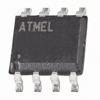
AT93C86-10SI-2.7 Atmel, AT93C86-10SI-2.7 Datasheet

AT93C86-10SI-2.7
Specifications of AT93C86-10SI-2.7
Available stocks
Related parts for AT93C86-10SI-2.7
AT93C86-10SI-2.7 Summary of contents
Page 1
... The AT93C86 is available in space saving 8-lead PDIP, 8-lead JEDEC SOIC and 8-lead TSSOP packages. The AT93C86 is enabled through the Chip Select pin (CS), and accessed via a 3-wire serial interface consisting of Data Input (DI), Data Output (DO), and Shift Clock (SK). ...
Page 2
... DO. The WRITE cycle is completely self-timed and no separate ERASE cycle is required before WRITE. The WRITE cycle is only enabled when the part is in the ERASE/WRITE ENABLE state. When CS is brought “high” following the initiation of a WRITE cycle, the DO pin outputs the READY/BUSY status of the part. The AT93C86 is available in a 2.7V to 5.5V version. ...
Page 3
... WRITE at 1.0 MHz 4. 4. -100 µA OH AT93C86 = +5.0V (unless otherwise noted). CC Max Units Conditions +2.7V to +5.5V, CC Min Typ Max 2.7 5.5 4.5 5.5 0.5 2.0 0.5 2.0 6.0 10 0.1 1.0 0.1 1 0.3 ...
Page 4
... PD1 t Output Delay to ‘0’ PD0 Status Valid High t DF Impedance t Write Cycle Time WP (1) Endurance 5.0V, 25°C, Page Mode Note: 1. This parameter is characterized and is not 100% tested. AT93C86 4 = -40° 85° Test Condition 4.5V V 5.5V CC 2.7V V 5.5V CC 4.5V V 5. ...
Page 5
... D 7 00XXXXXXXX The AT93C86 is accessed via a simple and versatile 3-wire serial communication inter- face. Device operation is controlled by seven instructions issued by the host processor. A valid instruction starts with a rising edge of CS and consists of a Start Bit (logic “1”) followed by the appropriate Op Code and the desired memory Address location. ...
Page 6
... AT93C86 6 ERASE ALL (ERAL): The Erase All (ERAL) instruction programs every bit in the mem- ory array to the logic “1” state and is primarily used for testing purposes. The DO pin outputs the READY/BUSY status of the part brought high after being kept low for a minimum of 250 ...
Page 7
... Timing Diagrams Synchronous Data Timing Note: 1. This is the minimum SK period. Organization Key for Timing Diagrams I 1237E–SEEPR–01/03 AT93C86 (16K AT93C86 ...
Page 8
... READ Timing High Impedance EWEN Timing EWDS Timing AT93C86 8 ... ... 1237E–SEEPR–01/03 ...
Page 9
... WRITE Timing HIGH IMPEDANCE DO (1) WRAL Timing HIGH IMPEDANCE DO Note: 1. Valid only 4.5V to 5.5V. CC 1237E–SEEPR–01/03 ... ... ... D AT93C86 t CS BUSY READY ... D0 N BUSY READY ...
Page 10
... ERASE Timing HIGH IMPEDANCE DO (1) ERAL Timing HIGH IMPEDANCE DO Note: 1. Valid only 4.5V to 5.5V. CC AT93C86 ... N-1 N STANDBY CHECK STATUS HIGH IMPEDANCE BUSY READY STANDBY CHECK STATUS BUSY HIGH IMPEDANCE READY t WP 1237E–SEEPR–01/03 ...
Page 11
... AT93C86 Ordering Information Ordering Code AT93C86-10PI-2.7 AT93C86-10SI-2.7 AT93C86-10TI-2.7 AT93C86-10SJ-2.7 AT93C86-10SE-2.7 Note: For 2.7V devices used in a 4.5V to 5.5V range, please refer to performance values in the AC and DC characteristics tables. 8P3 8-lead, 0.300" Wide, Plastic Dual Inline Package (PDIP) 8S1 8-lead, 0.150" Wide, Plastic Gull Wing Small Outline (JEDEC SOIC) 8A2 8-lead, 0.170" ...
Page 12
... D, D1 and E1 dimensions do not include mold Flash or protrusions. Mold Flash or protrusions shall not exceed 0.010 inch and eA measured with the leads constrained to be perpendicular to datum. 5. Pointed or rounded lead tips are preferred to ease insertion and b3 maximum dimensions do not include Dambar protrusions. Dambar protrusions shall not exceed 0.010 (0.25 mm). 2325 Orchard Parkway San Jose, CA 95131 R AT93C86 ...
Page 13
... This drawing is for general information only. Refer to JEDEC Drawing MS-012 for proper dimensions, tolerances, datums, etc. 2325 Orchard Parkway San Jose, CA 95131 R 1237E–SEEPR–01/ TITLE 8S1, 8-lead (0.150" Wide Body), Plastic Gull Wing Small Outline (JEDEC SOIC) AT93C86 COMMON DIMENSIONS (Unit of Measure = mm) SYMBOL MIN NOM MAX NOTE A – – 1.75 B – ...
Page 14
... Dimension b does not include Dambar protrusion. Allowable Dambar protrusion shall be 0.08 mm total in excess of the b dimension at maximum material condition. Dambar cannot be located on the lower radius of the foot. Minimum space between protrusion and adjacent lead is 0.07 mm. 5. Dimension D and determined at Datum Plane H. 2325 Orchard Parkway San Jose, CA 95131 R AT93C86 TITLE 8A2, 8-lead, 4 ...
Page 15
... No licenses to patents or other intellectual property of Atmel are granted by the Company in connection with the sale of Atmel products, expressly or by implication. Atmel’s products are not authorized for use as critical components in life support devices or systems. ...


