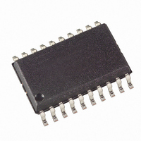
AT25P1024W1-10SI-2.7 Atmel, AT25P1024W1-10SI-2.7 Datasheet - Page 8

AT25P1024W1-10SI-2.7
Manufacturer Part Number
AT25P1024W1-10SI-2.7
Description
IC EEPROM 1MBIT 2.1MHZ 20SOIC
Manufacturer
Atmel
Datasheet
1.AT25P1024C1-10CI-1.8.pdf
(17 pages)
Specifications of AT25P1024W1-10SI-2.7
Format - Memory
EEPROMs - Serial
Memory Type
EEPROM
Memory Size
1M (128K x 8)
Speed
1MHz, 2.1MHz
Interface
SPI, 3-Wire Serial
Voltage - Supply
2.7 V ~ 5.5 V
Operating Temperature
-40°C ~ 85°C
Package / Case
20-SOIC (7.5mm Width)
Lead Free Status / RoHS Status
Contains lead / RoHS non-compliant
Other names
AT25P1024C10SI2.7
8
AT25P1024
Table 7. Read Status Register Bit Definition
WRITE STATUS REGISTER (WRSR): The WRSR instruction allows the user to select
one of four levels of protection. The AT25P1024 is divided into four array segments. Top
quarter (1/4), top half (1/2), or all of the memory segments can be protected. Any of the
data within any selected segment will therefore be read only. The block write protection
levels and corresponding status register control bits are shown in Table 8.
The three bits, BP0, BP1, and WPEN are nonvolatile cells that have the same properties
and functions as the regular memory cells (e.g. WREN, t
Table 8. Block Write Protect Bits
The WRSR instruction also allows the user to enable or disable the write protect (WP)
pin through the use of the write protect enable (WPEN) bit. Hardware write protection is
enabled when the WP pin is low and the WPEN bit is “1”. Hardware write protection is
disabled when either the WP pin is high or the WPEN bit is “0”. When the device is hard-
ware write protected, writes to the Status Register, including the block protect bits and
the WPEN bit, and the block-protected sections in the memory array are disabled.
Writes are only allowed to sections of the memory which are not block-protected.
NOTE: When the WPEN bit is hardware write protected, it cannot be changed back to
“0”, as long as the WP pin is held low.
Table 9. WPEN Operation
Bit
Bit 0 (RDY)
Bit 1 (WEN)
Bit 2 (BP0)
Bit 3 (BP1)
Bits 4-6 are “0”s when device is not in an internal write cycle.
Bit 7 (WPEN)
Bits 0-7 are “1”s during an internal write cycle.
Level
0
1(1/4)
2(1/2)
3(All)
WPEN
0
0
1
WP
Low
X
X
BP1
Status Register Bits
0
0
1
1
Definition
Bit 0 = “0” (RDY) indicates the device is ready. Bit 0 = “1” indicates the write cycle
is in progress.
Bit 1 = “0” indicates the device is not write enabled. Bit 1 = “1” indicates the device
is write enabled.
See Table 8.
See Table 8.
See Table 9.
WEN
0
1
0
BP0
0
1
0
1
Protected
Protected
Protected
Protected
Blocks
Unprotected Blocks
Array Addresses Protected
WC
Protected
Protected
Writable
, RDSR).
010000 - 01FFFF
01800 - 01FFFF
0000 - 01FFFF
AT25P1024
None
Status Register
1082I–SEEPR–7/06
Protected
Protected
Writable


