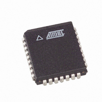
AT49BV040-15JC Atmel, AT49BV040-15JC Datasheet - Page 3

AT49BV040-15JC
Manufacturer Part Number
AT49BV040-15JC
Description
IC FLASH 4MBIT 150NS 32PLCC
Manufacturer
Atmel
Datasheet
1.AT49BV040-15JC.pdf
(12 pages)
Specifications of AT49BV040-15JC
Format - Memory
FLASH
Memory Type
FLASH
Memory Size
4M (512K x 8)
Speed
150ns
Interface
Parallel
Voltage - Supply
2.7 V ~ 3.6 V
Operating Temperature
0°C ~ 70°C
Package / Case
32-PLCC
Lead Free Status / RoHS Status
Contains lead / RoHS non-compliant
Other names
AT49BV04015JC
Once the feature is enabled, the data in the boot block can
no longer be erased or programmed. Data in the main
memory block can still be changed through the regular pro-
gramming method. To activate the lockout feature, a series
of six program commands to specific addresses with spe-
cific data must be performed. Please refer to the Com-
mand Definitions table.
BOOT BLOCK LOCKOUT DETECTION: A software
method is available to determine if programming of the boot
block section is locked out. When the device is in the soft-
ware product identification mode (see Software Product
Identification Entry and Exit sections) a read from address
location 00002H will show if programming the boot block is
locked out. If the data on I/O0 is low, the boot block can be
programmed; if the data on I/O0 is high, the program lock-
out feature has been activated and the block cannot be
programmed. The software product identification code
should be used to return to standard operation.
PRODUCT IDENTIFICATION: The product identification
mode identifies the device and manufacturer as Atmel.
It may be accessed by hardware or software operation.
The hardware operation mode can be used by an external
programmer to identify the correct programming algorithm
for the Atmel product.
For details, see Operating Modes (for hardware operation)
or Software Product Identification. The manufacturer and
device code is the same for both modes.
DATA POLLING: The AT49BV/LV040 features DATA poll-
ing to indicate the end of a program cycle. During a pro-
gram cycle an attempted read of the last byte loaded will
result in the complement of the loaded data on I/O7. Once
the program cycle has been completed, true data is valid
on all outputs and the next cycle may begin. DATA polling
may begin at any time during the program cycle.
TO G G L E B I T: I n a d d i t i o n t o D A T A p o l l i n g t h e
AT49BV/LV040 provides another method for determining
the end of a program or erase cycle. During a program or
erase operation, successive attempts to read data from the
device will result in I/O6 toggling between one and zero.
Once the program cycle has completed, I/O6 will stop tog-
gling and valid data will be read. Examining the toggle bit
may begin at any time during a program cycle.
HARDWARE DATA PROTECTION: Hardware features
protect against inadvertent programs to the AT49BV/LV040
in the following ways: (a) V
(typical), the program function is inhibited. (b) Program
inhibit: holding any one of OE low, CE high or WE high
inhibits program cycles. (c) Noise filter: pulses of less than
15 ns (typical) on the WE or CE inputs will not initiate a pro-
gram cycle.
INPUT LEVELS: While operating with a 2.7V to 3.6V
power supply, the address inputs and control inputs (OE,
CE and WE) may be driven from 0 to 5.5V without
adversely affecting the operation of the device. The I/O
l i n e s c a n o n l y b e d r i v e n f r o m 0 t o V C C + 0 . 6 V .
CC
sense: if V
CC
is below 1.8V
3


