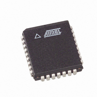
AT49BV001-90JI Atmel, AT49BV001-90JI Datasheet - Page 6

AT49BV001-90JI
Manufacturer Part Number
AT49BV001-90JI
Description
IC FLASH 1MBIT 120NS 32PLCC
Manufacturer
Atmel
Datasheet
1.AT49LV001-90JC.pdf
(25 pages)
Specifications of AT49BV001-90JI
Format - Memory
FLASH
Memory Type
FLASH
Memory Size
1M (128K x 8)
Speed
120ns
Interface
Parallel
Voltage - Supply
2.7 V ~ 3.6 V
Operating Temperature
-40°C ~ 85°C
Package / Case
32-PLCC
Lead Free Status / RoHS Status
Contains lead / RoHS non-compliant
Other names
AT49BV00190JI
Available stocks
Company
Part Number
Manufacturer
Quantity
Price
Company:
Part Number:
AT49BV001-90JI
Manufacturer:
ATM
Quantity:
5 530
Command Definition (in Hex)
Notes:
Absolute Maximum Ratings*
6
Command
Sequence
Read
Chip Erase
Sector Erase
Byte Program
Boot Block Lockout
Product ID Entry
Product ID Exit
Product ID Exit
Temperature Under Bias................................ -55°C to +125°C
Storage Temperature ..................................... -65°C to +150°C
All Input Voltages
(including NC Pins)
with Respect to Ground ...................................-0.6V to +6.25V
All Output Voltages
with Respect to Ground .............................-0.6V to V
Voltage on OE
with Respect to Ground ...................................-0.6V to +13.5V
1. The DATA FORMAT in each bus cycle is as follows: I/O7 - I/O0 (Hex)
2. The 16K byte boot sector has the address range 00000H to 03FFFH for the AT49BV/LV001(N) and
3. Either one of the Product ID Exit commands can be used.
4. SA = sector addresses:
AT49BV/LV001(N)(T)
1C000H to 1FFFFH for the AT49BV/LV001(N)T.
For the AT49BV/LV001(N):
SA = 00000 to 03FFF for BOOT BLOCK
Nothing will happen and the device goes back to the read mode in 100 ns
SA = 04000 to 05FFF for PARAMETER BLOCK 1
SA = 06000 to 07FFF for PARAMETER BLOCK 2
SA = 08000 to 0FFFF for MAIN MEMORY ARRAY BLOCK 1
This command will erase - PB1, PB2 and MMB1
SA = 10000 to 1FFFF for MAIN MEMORY ARRAY BLOCK 2
For the AT49BV/LV001(N)T:
SA = 1C000 to 1FFFF for BOOT BLOCK
Nothing will happen and the device goes back to the read mode in 100 ns
SA = 1A000 to 1BFFF for PARAMETER BLOCK 1
SA = 18000 to 19FFF for PARAMETER BLOCK 2
SA = 10000 to 17FFF for MAIN MEMORY ARRAY BLOCK 1
This command will erase - PB1, PB2 and MMB1
SA = 00000 to 0FFFF for MAIN MEMORY ARRAY BLOCK 2
(3)
(3)
(2)
Cycles
Bus
1
6
6
4
6
3
3
1
XXXX
Addr
5555
5555
5555
5555
5555
5555
Addr
1st Bus
Cycle
Data
D
AA
AA
AA
AA
AA
AA
F0
OUT
(1)
CC
2AAA
2AAA
2AAA
2AAA
2AAA
2AAA
Addr
2nd Bus
+ 0.6V
Cycle
Data
55
55
55
55
55
55
*NOTICE:
Addr
5555
5555
5555
5555
5555
5555
3rd Bus
Cycle
Data
80
80
A0
80
90
F0
Stresses beyond those listed under “Absolute Maxi-
mum Ratings” may cause permanent damage to the
device. This is a stress rating only and functional
operation of the device at these or any other condi-
tions beyond those indicated in the operational sec-
tions of this specification is not implied. Exposure to
absolute maximum rating conditions for extended
periods may affect device reliability.
Addr
5555
5555
5555
Addr
4th Bus
Cycle
Data
AA
D
AA
AA
IN
2AAA
2AAA
2AAA
Addr
5th Bus
Cycle
Data
55
55
55
1110C–FLASH–9/03
Addr
5555
SA
5555
6th Bus
(4)
Cycle
Data
10
30
40


