AT29C257-20JI Atmel, AT29C257-20JI Datasheet - Page 3
AT29C257-20JI
Manufacturer Part Number
AT29C257-20JI
Description
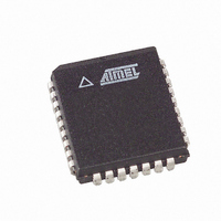
IC FLASH 256KBIT 200NS 32PLCC
Manufacturer
Atmel
Datasheet
1.AT29C257-12JI.pdf
(12 pages)
Specifications of AT29C257-20JI
Format - Memory
FLASH
Memory Type
FLASH
Memory Size
256K (32K x 8)
Speed
200ns
Interface
Parallel
Voltage - Supply
4.5 V ~ 5.5 V
Operating Temperature
-40°C ~ 85°C
Package / Case
32-PLCC
Lead Free Status / RoHS Status
Contains lead / RoHS non-compliant
Other names
AT29C25720JI
Available stocks
Company
Part Number
Manufacturer
Quantity
Price
Company:

Part Number:
AT29C257-20JI
Manufacturer:
ATM
Quantity:
2 400
Company:
Part Number:
AT29C257-20JI
Manufacturer:
ATM
Quantity:
2 400


Device Operation (Continued)
HARDWARE DATA PROTECTION:
protect against inadvertent programs to the AT29C257 in
the following ways: (a) V
(typical), the program function is inhibited. (b) V
on delay— once V
the device will automatically time out 5 ms (typical) before
programming. (c) Program inhibit— holding any one of OE
low, CE high or WE high inhibits program cycles. (d) Noise
filter— pulses of less than 15 ns (typical) on the WE or CE
inputs will not initiate a program cycle.
PRODUCT IDENTIFICATION: The product identifica-
tion mode identifies the device and manufacturer and may
be accessed by a hardware or software operation. For de-
tails, see Operating Modes or Software Product Identifica-
tion.
Absolute Maximum Ratings*
Temperature Under Bias................. -55 C to +125 C
Storage Temperature...................... -65 C to +150 C
All Input Voltages
(including NC Pins)
with Respect to Ground ................... -0.6V to +6.25V
All Output Voltages
with Respect to Ground .............-0.6V to V
Voltage on OE
with Respect to Ground ................... -0.6V to +13.5V
CC
has reached the V
CC
sense— if V
Hardware features
CC
CC
is below 3.8V
CC
sense level,
CC
+ 0.6V
power
DATA POLLING:
ing to indicate the end of a program cycle. During a pro-
gram cycle an attempted read of the last byte loaded will
result in the complement of the loaded data on I/O7. Once
the program cycle has been completed, true data is valid
on all outputs and the next cycle may begin. DATA polling
may begin at any time during the program cycle.
TOGGLE BIT:
AT29C257 provides another method for determining the
end of a program or erase cycle. During a program or
erase operation, successive attempts to read data from
the device will result in I/O6 toggling between one and
zero. Once the program cycle has completed, I/O6 will
stop toggling and valid data will be read. Examining the
toggle bit may begin at any time during a program cycle.
OPTIONAL CHIP ERASE MODE: The entire device
can be erased by using a 6-byte software code. Please
see Software Chip Erase application note for details.
*NOTICE: Stresses beyond those listed under “Absolute Maxi-
mum Ratings” may cause permanent damage to the device.
This is a stress rating only and functional operation of the
device at these or any other conditions beyond those indi-
cated in the operational sections of this specification is not
implied. Exposure to absolute maximum rating conditions
for extended periods may affect device reliability.
I n a d d i t i o n t o DATA p o l l i n g t h e
The AT29C257 features DATA poll-
AT29C257
4-107
Related parts for AT29C257-20JI
Image
Part Number
Description
Manufacturer
Datasheet
Request
R

Part Number:
Description:
357-036-542-201 CARDEDGE 36POS DL .156 BLK LOPRO
Manufacturer:
ATMEL Corporation
Datasheet:

Part Number:
Description:
IC FLASH 256KBIT 120NS 32PLCC
Manufacturer:
Atmel
Datasheet:
Part Number:
Description:
IC FLASH 256KBIT 200NS 32PLCC
Manufacturer:
Atmel
Datasheet:
Part Number:
Description:
IC FLASH 256KBIT 70NS 32PLCC
Manufacturer:
Atmel
Datasheet:
Part Number:
Description:
IC FLASH 256KBIT 90NS 32PLCC
Manufacturer:
Atmel
Datasheet:
Part Number:
Description:
IC FLASH 256KBIT 90NS 32PLCC
Manufacturer:
Atmel
Datasheet:

Part Number:
Description:
256K 32K x 8 5-volt Only CMOS Flash Memory
Manufacturer:
ATMEL [ATMEL Corporation]
Datasheet:
Part Number:
Description:
IC FLASH 256KBIT 150NS 32PLCC
Manufacturer:
Atmel
Datasheet:
Part Number:
Description:
IC FLASH 256KBIT 70NS 32PLCC
Manufacturer:
Atmel
Datasheet:
Part Number:
Description:
256k 32k X 8 5-volt Only Cmos Flash Memory
Manufacturer:
ATMEL Corporation
Datasheet:
Part Number:
Description:
256K 32K x 8 5-volt Only CMOS Flash Memory
Manufacturer:
ATMEL Corporation
Datasheet:

Part Number:
Description:
flash, Flash, Memory, Semiconductors and Actives, ic, cmos
Manufacturer:
Atmel
Datasheet:

Part Number:
Description:
DEV KIT FOR AVR/AVR32
Manufacturer:
Atmel
Datasheet: