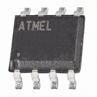
AT25160N-10SI Atmel, AT25160N-10SI Datasheet

AT25160N-10SI
Specifications of AT25160N-10SI
Available stocks
Related parts for AT25160N-10SI
AT25160N-10SI Summary of contents
Page 1
Features • Serial Peripheral Interface (SPI) Compatible • Supports SPI Modes 0 (0,0) and 3 (1,1) • Low-voltage and Standard-voltage Operation – 2 2.7V to 5.5V) CC – 1 1.8V to 5.5V) CC • 3.0 MHz ...
Page 2
BLOCK WRITE protection is enabled by programming the status register with one of four blocks of write protection. Sepa- rate program enable and program disable instructions are provided for additional data protection. Hardware data protection is provided via the WP ...
Page 3
Pin Capacitance Applicable over recommended operating range from T Symbol Test Conditions C Output Capacitance (SO) OUT C Input Capacitance(CS, SCK, SI, WP, HOLD) IN Note: 1. This parameter is characterized and is not 100% tested. (1) DC Characteristics ...
Page 4
AC Characteristics Applicable over recommended operating range from T 100 pF (unless otherwise noted). Symbol Parameter f SCK Clock Frequency SCK t Input Rise Time RI t Input Fall Time FI t SCK High Time WH t SCK Low Time ...
Page 5
AC Characteristics (Continued) Applicable over recommended operating range from T 100 pF (unless otherwise noted). Symbol Parameter t Hold to Output Low Hold to Output High Output Disable Time DIS t Write Cycle Time ...
Page 6
Serial Interface MASTER: The device that generates the serial clock. Description SLAVE: Because the Serial Clock pin (SCK) is always an input, the AT25080/160/320/640 always operates as a slave. TRANSMITTER/RECEIVER: The AT25080/160/320/640 has separate pins designated for data transmission (SO) ...
Page 7
SPI Serial Interface 0675M–SEEPR–9/03 AT25080/160/320/640 7 ...
Page 8
... Set Write Enable Latch 0000 X100 Reset Write Enable Latch 0000 X101 Read Status Register 0000 X001 Write Status Register 0000 X011 Read Data from Memory Array 0000 X010 Write Data to Memory Array Bit 6 Bit 5 Bit 4 Bit BP1 Definition Bit (RDY) indicates the device is READY. Bit indicates the write cycle is in progress ...
Page 9
... WRITE STATUS REGISTER (WRSR): The WRSR instruction allows the user to select one of four levels of protection. The AT25080/160/320/640 is divided into four array segments. One quarter (1/4), one half (1/2), or all of the memory segments can be protected. Any of the data within any selected segment will therefore be READ only. The block write protection levels and corresponding status register control bits are shown in Table 4 ...
Page 10
... First, the device must be write enabled via the Write Enable (WREN) Instruction. Then a Write (WRITE) Instruction may be executed. Also, the address of the memory location( programmed must be outside the protected address field location selected by the Block Write Protection Level. During an internal write cycle, all commands will be ignored except the RDSR instruction ...
Page 11
Timing Diagrams Synchronous Data Timing (for Mode CSS V IH SCK HI WREN Timing WRDI Timing 0675M–SEEPR–9/ ...
Page 12
RDSR Timing CS 0 SCK INSTRUCTION SI HIGH IMPEDANCE SO WRSR Timing CS 0 SCK SI HIGH IMPEDANCE SO READ Timing SCK SI INSTRUCTION HIGH IMPEDANCE SO AT25080/160/320/640 ...
Page 13
WRITE Timing SCK INSTRUCTION SI HIGH IMPEDANCE SO HOLD Timing CS SCK 0675M–SEEPR–9/ ...
Page 14
AT25080 Ordering Information Ordering Code AT25080-10PI-2.7 AT25080N-10SI-2.7 AT25080T1-10TI-2.7 AT25080-10PI-1.8 AT25080N-10SI-1.8 AT25080T1-10TI-1.8 Note: For 2.7V devices used in the 4.5V to 5.5V range, please refer to performance values in the AC and DC Characteristics tables. 8P3 8-lead, 0.300" Wide, Plastic Dual ...
Page 15
... AT25160 Ordering Information Ordering Code AT25160-10PI-2.7 AT25160N-10SI-2.7 AT25160T1-10TI-2.7 AT25160-10PI-1.8 AT25160N-10SI-1.8 AT25160T1-10TI-1.8 Note: For 2.7V devices used in the 4.5V to 5.5V range, please refer to performance values in the AC and DC Characteristics tables. 8P3 8-lead, 0.300" Wide, Plastic Dual Inline Package (PDIP) 8S1 8-lead, 0.150" Wide, Plastic Gull Wing Small Outline (JEDEC SOIC) 14A2 14-lead, 0.170" ...
Page 16
AT25320 Ordering Information Ordering Code AT25320-10PI-2.7 AT25320N-10SI-2.7 AT25320T1-10TI-2.7 Note: For 2.7V devices used in the 4.5V to 5.5V range, please refer to performance values in the AC and DC Characteristics tables. 8P3 8-lead, 0.300" Wide, Plastic Dual Inline Package (PDIP) ...
Page 17
AT25640 Ordering Information Ordering Code AT25640-10PI-2.7 AT25640N-10SI-2.7 AT25640T1-10TI-2.7 AT25640-10PI-1.8 AT25640N-10SI-1.8 AT25640T1-10TI-1.8 Note: For 2.7V devices used in the 4.5V to 5.5V range, please refer to performance values in the AC and DC Characteristics tables. 8P3 8-lead, 0.300" Wide, Plastic Dual ...
Page 18
Packaging Information 8P3 – PDIP Top View PLCS Side View Notes: 1. This drawing is for general information only; refer to JEDEC Drawing MS-001, Variation BA for additional information. 2. Dimensions A and L are measured ...
Page 19
JEDEC SOIC Top View e Side View Note: These drawings are for general information only. Refer to JEDEC Drawing MS-012, Variation AA for proper dimensions, tolerances, datums, etc. 1150 E. Cheyenne Mtn. Blvd. Colorado Springs, CO 80906 R ...
Page 20
TSSOP Top View D A Side View Notes: 1. This drawing is for general information only. Please refer to JEDEC Drawing MO-153, Variation AB-1, for additional information. 2. Dimension D does not include mold ...
Page 21
... No licenses to patents or other intellectual property of Atmel are granted by the Company in connection with the sale of Atmel products, expressly or by implication. Atmel’s products are not authorized for use as critical components in life support devices or systems. ...


