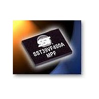
SST39VF400A-70-4I-B3KE Microchip Technology, SST39VF400A-70-4I-B3KE Datasheet - Page 18

SST39VF400A-70-4I-B3KE
Manufacturer Part Number
SST39VF400A-70-4I-B3KE
Description
IC FLASH MPF 4MBIT 70NS 48TFBGA
Manufacturer
Microchip Technology
Datasheets
1.SST39VF010-70-4C-NHE.pdf
(2 pages)
2.SST39VF010-70-4C-NHE.pdf
(2 pages)
3.SST39VF400A-70-4C-B3KE.pdf
(31 pages)
Specifications of SST39VF400A-70-4I-B3KE
Memory Type
FLASH
Memory Size
4M (256K x 16)
Operating Temperature
-40°C ~ 85°C
Package / Case
48-TFBGA
Format - Memory
FLASH
Speed
70ns
Interface
Parallel
Voltage - Supply
2.7 V ~ 3.6 V
Data Bus Width
16 bit
Architecture
Sectored
Interface Type
CFI
Access Time
70 ns
Supply Voltage (max)
3.6 V
Supply Voltage (min)
2.7 V
Maximum Operating Current
30 mA
Mounting Style
SMD/SMT
Organization
256 KB x 16
Memory Configuration
256K X 16
Ic Interface Type
Parallel
Clock Frequency
14MHz
Supply Voltage Range
2.7V To 3.6V
Memory Case Style
BGA
Lead Free Status / RoHS Status
Lead free / RoHS Compliant
Lead Free Status / RoHS Status
Lead free / RoHS Compliant, Lead free / RoHS Compliant
Available stocks
Company
Part Number
Manufacturer
Quantity
Price
Company:
Part Number:
SST39VF400A-70-4I-B3KE
Manufacturer:
Microchip Technology
Quantity:
10 000
Part Number:
SST39VF400A-70-4I-B3KE
Manufacturer:
SST
Quantity:
20 000
Company:
Part Number:
SST39VF400A-70-4I-B3KE-T
Manufacturer:
Microchip Technology
Quantity:
10 000
Data Sheet
©2010 Silicon Storage Technology, Inc.
ADDRESS A
ADDRESS A
FIGURE 11: WE# Controlled Block-Erase Timing Diagram
FIGURE 12: WE# Controlled Sector-Erase Timing Diagram
DQ
DQ
WE#
MS-0
WE#
OE#
MS-0
CE#
OE#
CE#
15-0
15-0
Note: This device also supports CE# controlled Block-Erase operation. The WE# and CE# signals are
Note: This device also supports CE# controlled Sector-Erase operation. The WE# and CE# signals are
5555
interchageable as long as minimum timings are met. (See Table 16)
BA
A
5555
interchageable as long as minimum timings are met. (See Table 16)
SA
A
MS
A
X can be V
XXAA
MS
A
X can be V
SW0
T
X
MS
XXAA
X
MS
T
SW0
WP
= Block Address
= Most significant address
= Sector Address
WP
= Most significant address
= A
= A
16
16
2AAA
IL
2AAA
for SST39LF/VF200A, A
IL
for SST39LF/VF200A, A
or V
XX55
or V
SW1
XX55
SW1
SIX-BYTE CODE FOR BLOCK-ERASE
SIX-BYTE CODE FOR SECTOR-ERASE
IH
IH
, but no other value.
, but no other value.
5555
5555
XX80
SW2
XX80
SW2
SST39VF200A / SST39VF400A / SST39VF800A
17
SST39LF200A / SST39LF400A / SST39LF800A
17
5555
5555
for SST39LF/VF400A and A
for SST39LF/VF400A and A
XXAA
SW3
2 Mbit / 4 Mbit / 8 Mbit Multi-Purpose Flash
XXAA
SW3
18
2AAA
2AAA
XX55
SW4
XX55
SW4
BA
18
XX50
18
SW5
SA
XX30
SW5
for SST39LF/VF800A
X
for SST39LF/VF800A
X
T
T
BE
SE
S71117-13-000
1117 F17.9
1117 F18.8
11/10


