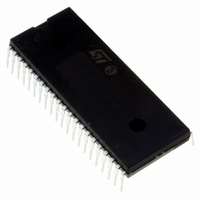
M27C160-100B1 STMicroelectronics, M27C160-100B1 Datasheet - Page 8

M27C160-100B1
Manufacturer Part Number
M27C160-100B1
Description
IC OTP 16MBIT 100NS 42DIP
Manufacturer
STMicroelectronics
Datasheet
1.M27C160-100B1.pdf
(26 pages)
Specifications of M27C160-100B1
Format - Memory
EPROMs
Memory Type
OTP EPROM
Memory Size
16M (2M x 8 or 1M x 16)
Speed
100ns
Interface
Parallel
Voltage - Supply
4.5 V ~ 5.5 V
Operating Temperature
0°C ~ 70°C
Package / Case
42-DIP (0.600", 15.24mm)
Lead Free Status / RoHS Status
Lead free / RoHS Compliant
Available stocks
Company
Part Number
Manufacturer
Quantity
Price
Device description
2
Note:
2.1
2.2
8/26
Read mode
Standby mode
Device description
Table 2
read mode. All inputs are TTL compatible except for V
Signature.
Table 2.
X = V
The M27C160 has two organisations, Word-wide and Byte-wide. The organisation is
selected by the signal level on the BYTEV
organisation is selected and the Q15A–1 pin is used for Q15 Data Output. When the
BYTEV
the Address Input A–1. When the memory is logically regarded as 16 bit wide, but read in
the Byte-wide organisation, then with A–1 at V
selected and with A–1 at V
The M27C160 has two control functions, both of which must be logically active in order to
obtain data at the outputs. In addition the Word-wide or Byte- wide organisation must be
selected.
Chip Enable (E) is the power control and should be used for device selection. Output Enable
(G) is the output control and should be used to gate data to the output pins independent of
device selection. Assuming that the addresses are stable, the address access time (t
is equal to the delay from E to output (t
t
been stable for at least t
The M27C160 has a standby mode which reduces the active current from 50mA to 100µA.
The M27C160 is placed in the standby mode by applying a CMOS high signal to the E input.
Read Word-wide
Read Byte-wide Upper
Read Byte-wide Lower
Output Disable
Program
Verify
Program Inhibit
Standby
Electronic Signature
GLQV
IH
from the falling edge of G, assuming that E has been low and the addresses have
PP
or V
lists the operating modes of the M27C160. A single power supply is required in the
Mode
pin is at V
IL
, V
Operating Modes
ID
= 12V ± 0.5V.
IL
the Byte-wide organisation is selected and the Q15A–1 pin is used for
V
AVQV
IL
V
V
V
V
V
V
V
V
Pulse
E
IH
IH
IH
IH
IL
IL
IL
IL
IL
-t
the upper 8 bits of the 16 bit data are selected.
GLQV
.
V
V
V
V
V
V
V
V
G
X
IH
IH
IH
IL
IL
IL
IL
IL
ELQV
PP
BYTEV
). Data is available at the output after a delay of
V
V
V
V
V
pin. When BYTEV
V
V
X
X
PP
PP
PP
IH
IH
IL
IL
IL
the lower 8 bits of the 16 bit data are
PP
PP
V
A9
X
X
X
X
X
X
X
X
ID
and 12V on A9 for the Electronic
Data Out
Data Out
Q15A–1
Data In
Code
PP
Hi-Z
Hi-Z
Hi-Z
V
V
IH
IL
is at V
Data Out
Data Out
Q8-Q14
Data In
IH
Codes
Hi-Z
Hi-Z
Hi-Z
Hi-Z
Hi-Z
the Word-wide
M27C160
Data Out
Data Out
Data Out
Data Out
Data In
Q7-Q0
Codes
Hi-Z
Hi-Z
Hi-Z
AVQV
)


