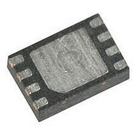
M45PE20-VMP6G NUMONYX, M45PE20-VMP6G Datasheet - Page 15

M45PE20-VMP6G
Manufacturer Part Number
M45PE20-VMP6G
Description
IC FLASH 2MBIT 75MHZ 8VFQFPN
Manufacturer
NUMONYX
Series
Forté™r
Datasheets
1.M45PE20-VMN6TP.pdf
(47 pages)
2.M45PE20-VMN6P.pdf
(34 pages)
3.M45PE20-VMP6G.pdf
(36 pages)
Specifications of M45PE20-VMP6G
Format - Memory
FLASH
Memory Type
FLASH
Memory Size
2M (256K x 8)
Speed
75MHz
Interface
SPI, 3-Wire Serial
Voltage - Supply
2.7 V ~ 3.6 V
Operating Temperature
-40°C ~ 85°C
Package / Case
8-VFQFN, 8-VFQFPN
Memory Configuration
256K X 8
Ic Interface Type
Serial, SPI
Clock Frequency
25MHz
Supply Voltage Range
2.7V To 3.6V
Memory Case Style
VDFPN
No. Of Pins
8
Interface Type
Serial, SPI
Rohs Compliant
Yes
Lead Free Status / RoHS Status
Lead free / RoHS Compliant
Available stocks
Company
Part Number
Manufacturer
Quantity
Price
Part Number:
M45PE20-VMP6G
Manufacturer:
ST
Quantity:
20 000
Read Data Bytes (READ)
The device is first selected by driving Chip Select
(S) Low. The instruction code for the Read Data
Bytes (READ) instruction is followed by a 3-byte
address (A23-A0), each bit being latched-in during
the rising edge of Serial Clock (C). Then the mem-
ory contents, at that address, is shifted out on Se-
rial Data Output (Q), each bit being shifted out, at
a maximum frequency f
Serial Clock (C).
The instruction sequence is shown in
The first byte addressed can be at any location.
The address is automatically incremented to the
Figure 11. Read Data Bytes (READ) Instruction Sequence and Data-Out Sequence
Note: Address bits A23 to A18 are Don’t Care.
S
C
D
Q
0
1
High Impedance
R
2
Instruction
, during the falling edge of
3
4
5
6
Figure
7
MSB
23
8
22 21
9 10
11..
24-Bit Address
3
28 29 30 31 32 33 34 35
next higher address after each byte of data is shift-
ed out. The whole memory can, therefore, be read
with a single Read Data Bytes (READ) instruction.
When the highest address is reached, the address
counter rolls over to 000000h, allowing the read
sequence to be continued indefinitely.
The Read Data Bytes (READ) instruction is termi-
nated by driving Chip Select (S) High. Chip Select
(S) can be driven High at any time during data out-
put. Any Read Data Bytes (READ) instruction,
while an Erase, Program or Write cycle is in
progress, is rejected without having any effects on
the cycle that is in progress.
2
1
0
MSB
7
6
5
Data Out 1
4
3
36 37 38
2
1
39
0
7
Data Out 2
AI03748D
M45PE20
15/35


