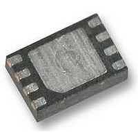
M25P20-VMP6G NUMONYX, M25P20-VMP6G Datasheet - Page 38

M25P20-VMP6G
Manufacturer Part Number
M25P20-VMP6G
Description
IC FLASH 2MBIT 50MHZ 8VFQFPN
Manufacturer
NUMONYX
Series
Forté™r
Specifications of M25P20-VMP6G
Format - Memory
FLASH
Memory Type
FLASH
Memory Size
2M (256K x 8)
Speed
50MHz
Interface
SPI, 3-Wire Serial
Voltage - Supply
2.7 V ~ 3.6 V
Operating Temperature
-40°C ~ 85°C
Package / Case
8-VFQFN, 8-VFQFPN
Clock Frequency
50MHz
Supply Voltage Range
2.7V To 3.6V
Memory Case Style
VDFPN
No. Of Pins
8
Base Number
25
Frequency
50MHz
Ic Generic Number
25P20
Memory Configuration
256K X 8
Interface Type
Serial, SPI
Rohs Compliant
Yes
Lead Free Status / RoHS Status
Lead free / RoHS Compliant
Available stocks
Company
Part Number
Manufacturer
Quantity
Price
Company:
Part Number:
M25P20-VMP6G
Manufacturer:
Micron Technology Inc
Quantity:
10 000
Part Number:
M25P20-VMP6G
Manufacturer:
ST
Quantity:
20 000
Company:
Part Number:
M25P20-VMP6GB
Manufacturer:
MICRON
Quantity:
5 600
38/55
Table 14.
2. This is preliminary data
Table 15.
1. Technology T9HX devices are identified by process identification digit "4" in the device marking and
2. When using the Page Program (PP) instruction to program consecutive Bytes, optimized timings are
,
Table 16.
1. Technology T7Y devices are identified by process identification digit "X" in the device marking.
Symbol
, Pro
Symbol
Symbol
I
I
I
I
I
I
I
V
t
V
V
process letter "B" in the part number.
obtained with one sequence including all Bytes, not several sequences of only a few Bytes (1 ≤ n ≤ 256).
I
CC1
CC2
CC3
CC4
CC5
CC6
CC7
V
PP
I
t
t
LO
OH
t
t
OL
LI
SE
BE
IH
W
W
IL
(2)
Input Leakage Current
Output Leakage Current
Standby Current
Deep Power-down Current
Operating Current (READ)
Operating Current (PP)
Operating Current (WRSR)
Operating Current (SE)
Operating Current (BE)
Input Low Voltage
Input High Voltage
Output Low Voltage
Output High Voltage
Alt.
DC Characteristics (Device Grade 3)
Instruction Times, process technology T9HX
Instruction Times, process technology T7Y, Device Grade 6
Alt.
Write Status Register Cycle Time
Page Program Cycle Time (256 Bytes)
Page Program Cycle Time (n Bytes)
Sector Erase Cycle Time
Bulk Erase Cycle Time
Parameter
Write Status Register Cycle Time
Test conditions specified in
Test conditions specified in
Parameter
Parameter
C = 0.1V
C = 0.1V
Test Condition (in addition to
S = V
S = V
those in
CC
CC
CC
CC
I
OH
I
OL
, V
, V
Q = open
Q = open
Table 10
Table 10
S = V
S = V
S = V
S = V
/ 0.9.V
/ 0.9.V
= –100 μA
= 1.6 mA
IN
IN
Table 10
= V
= V
CC
CC
CC
CC
CC
CC
Min.
SS
SS
at 25MHz,
at 20MHz,
and
and
or V
or V
)
Min.
(1)
int(n/8) × 0.025
Table 18
CC
CC
Table 18
(Device Grade 6)
Typ.
1.3
0.8
0.6
2.5
0.7V
Min.
Typ.
V
– 0.5
0.2
5
CC
CC
(1)
–
(1)
V
Max.
0.3V
Max.
CC
15
100
± 2
± 2
0.4
Max.
50
15
15
15
15
8
4
15
+0.4
5
3
6
CC
(1)
Unit
ms
Unit
Unit
mA
mA
mA
mA
mA
mA
ms
ms
µA
µA
µA
µA
V
V
V
V
s
s


