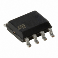
M25P10-AVMN6TP NUMONYX, M25P10-AVMN6TP Datasheet - Page 38

M25P10-AVMN6TP
Manufacturer Part Number
M25P10-AVMN6TP
Description
IC FLASH 1MBIT 50MHZ 8SOIC
Manufacturer
NUMONYX
Series
Forté™r
Datasheet
1.M25P10-AVMP6TG.pdf
(51 pages)
Specifications of M25P10-AVMN6TP
Format - Memory
FLASH
Memory Type
FLASH
Memory Size
1M (128K x 8)
Speed
50MHz
Interface
SPI, 3-Wire Serial
Voltage - Supply
2.3 V ~ 3.6 V
Operating Temperature
-40°C ~ 85°C
Package / Case
8-SOIC (3.9mm Width)
Package
8SO N
Cell Type
NOR
Density
1 Mb
Architecture
Sectored
Block Organization
Symmetrical
Typical Operating Supply Voltage
3.3 V
Sector Size
256Byte x 512
Timing Type
Synchronous
Interface Type
Serial-SPI
Lead Free Status / RoHS Status
Lead free / RoHS Compliant
Other names
M25P10-AVMN6TPTR
Available stocks
Company
Part Number
Manufacturer
Quantity
Price
Company:
Part Number:
M25P10-AVMN6TP
Manufacturer:
MICRON
Quantity:
11 200
Company:
Part Number:
M25P10-AVMN6TP
Manufacturer:
Numonyx
Quantity:
47 500
Company:
Part Number:
M25P10-AVMN6TP
Manufacturer:
ST
Quantity:
144
Company:
Part Number:
M25P10-AVMN6TP
Manufacturer:
MICRON85
Quantity:
4 940
Part Number:
M25P10-AVMN6TP
Manufacturer:
ST
Quantity:
20 000
38/51
Table 15.
1. Only for products with process technology code X.
2. Preliminary data.
Table 16.
1. When using the Page Program (PP) instruction to program consecutive bytes, optimized timings are
2. t
Symbol
Symbol
t
I
I
I
I
I
I
I
V
V
PP
V
I
CC1
CC2
CC3
CC4
CC5
CC6
CC7
t
t
V
obtained with one sequence including all the bytes versus several sequences of only a few bytes. (1 ≤ n ≤
256).
t
I
LO
SE
BE
PP
OH
W
LI
OL
IH
IL
(1)
=2
μ
s+8
Input Leakage current
Output Leakage current
Standby current
Deep Power-down current
Operating current (READ)
Operating current (PP)
Operating current (WRSR)
Operating current (SE)
Operating current (BE)
Input Low voltage
Input High voltage
Output Low voltage
Output High voltage
Alt.
μ
DC characteristics (device grade 3)
Instruction times (device grade 6)
s*[int(n-1)/2+1]+4
Write Status Register cycle time
Page Program cycle time (256 bytes)
Page Program cycle time (n bytes)
Sector Erase cycle time
Bulk Erase cycle time
Parameter
Test conditions specified in
μ
s*[int(n-1)/2]+2
Parameter
C = 0.1V
C = 0.1V
Test condition (in addition to
S = V
S = V
μ
s, in products with process technology code X and Y.
those in
CC
CC
CC
CC
I
OH
I
OL
, V
, V
Q = open
Q = open
/ 0.9.V
/ 0.9.V
S = V
S = V
S = V
S = V
= –100 μA
= 1.6 mA
Table 10
IN
IN
(1)
Table
= V
= V
CC
CC
CC
CC
CC
CC
SS
SS
at 25 MHz,
at 20 MHz,
10)
Min
or V
or V
and
CC
CC
Table 12
n*1/256
0.4+
0.65
Typ
1.4
1.7
V
5
0.7V
Min
CC
–0.5
(2)
–0.2
(2)
CC
V
Max
0.3V
Max
15
CC
5
3
6
100
± 2
± 2
0.4
50
15
15
15
15
8
4
+0.4
(2)
CC
Unit
ms
ms
Unit
s
s
mA
mA
mA
mA
mA
mA
μA
μA
μA
μA
V
V
V
V


