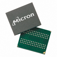
MT48LC4M32B2B5-6:G Micron Technology Inc, MT48LC4M32B2B5-6:G Datasheet - Page 21

MT48LC4M32B2B5-6:G
Manufacturer Part Number
MT48LC4M32B2B5-6:G
Description
IC SDRAM 128MBIT 167MHZ 90VFBGA
Manufacturer
Micron Technology Inc
Type
SDRAMr
Datasheet
1.MT48LC4M32B2P-7G_TR.pdf
(67 pages)
Specifications of MT48LC4M32B2B5-6:G
Format - Memory
RAM
Memory Type
SDRAM
Memory Size
128M (4Mx32)
Speed
167MHz
Interface
Parallel
Voltage - Supply
3 V ~ 3.6 V
Operating Temperature
0°C ~ 70°C
Package / Case
90-VFBGA
Organization
4Mx32
Density
128Mb
Address Bus
14b
Access Time (max)
17/7.5/5.5ns
Maximum Clock Rate
166MHz
Operating Supply Voltage (typ)
3.3V
Package Type
VFBGA
Operating Temp Range
0C to 70C
Operating Supply Voltage (max)
3.6V
Operating Supply Voltage (min)
3V
Supply Current
195mA
Pin Count
90
Mounting
Surface Mount
Operating Temperature Classification
Commercial
Package
90VFBGA
Address Bus Width
14 Bit
Operating Supply Voltage
3.3 V
Maximum Random Access Time
17|7.5|5.5 ns
Lead Free Status / RoHS Status
Lead free / RoHS Compliant
Available stocks
Company
Part Number
Manufacturer
Quantity
Price
Company:
Part Number:
MT48LC4M32B2B5-6:G
Manufacturer:
MICRON
Quantity:
2 400
Company:
Part Number:
MT48LC4M32B2B5-6:G
Manufacturer:
Micron Technology Inc
Quantity:
10 000
Part Number:
MT48LC4M32B2B5-6:G
Manufacturer:
MICRON/美光
Quantity:
20 000
Company:
Part Number:
MT48LC4M32B2B5-6:G TR
Manufacturer:
Micron Technology Inc
Quantity:
10 000
Figure 7:
READs
Figure 8:
PDF: 09005aef80872800/Source: 09005aef80863355
128MbSDRAMx32_2.fm - Rev. L 1/09 EN
Example: Meeting
READ Command
Notes:
COMMAND
1.
READ bursts are initiated with a READ command, as shown in Figure 8.
The starting column and bank addresses are provided with the READ command, and
auto precharge is either enabled or disabled for that burst access. If auto precharge is
enabled, the row being accessed is precharged at the completion of the burst. For the
generic READ commands used in the following illustrations, auto precharge is disabled.
During READ bursts, the valid data-out element from the starting column address will
be available following the CL after the READ command. Each subsequent data-out
element will be valid by the next positive clock edge. Figure 9 on page 22 shows general
timing for each possible CL setting.
A8, A9, A11
t
t
where x = number of clocks for equation to be true.
A0–A7
RCD (MIN) = 20ns,
RCD (MIN) ×
BA0,1
RAS#
CAS#
CLK
WE#
CKE
A10
CLK
CS#
t
RCD (MIN) When 2 <
HIGH
ACTIVE
T0
t
CK
DISABLE AUTO PRECHARGE
ENABLE AUTO PRECHARGE
t CK
t
CK = 8ns
COLUMN
ADDRESS
ADDRESS
BANK
t
t RCD (MIN) +0.5 t CK
NOP
RCD (MIN)
DON’T CARE
T1
21
t
RCD (MIN)/
t CK
Micron Technology, Inc., reserves the right to change products or specifications without notice.
NOP
T2
t
CK< 3
t CK
READ or
WRITE
DON’T CARE
T3
©2001 Micron Technology, Inc. All rights reserved.
128Mb: x32 SDRAM
Register Definition


