S-93C66BD0I-T8T1G Seiko Instruments, S-93C66BD0I-T8T1G Datasheet - Page 13

S-93C66BD0I-T8T1G
Manufacturer Part Number
S-93C66BD0I-T8T1G
Description
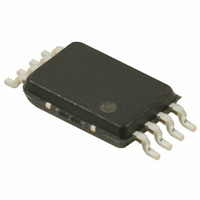
IC EEPROM 4KBIT 500KHZ 8TSSOP
Manufacturer
Seiko Instruments
Datasheet
1.S-93C46BD0I-T8T1G.pdf
(50 pages)
Specifications of S-93C66BD0I-T8T1G
Format - Memory
EEPROMs - Serial
Memory Type
EEPROM
Memory Size
4K (256 x 16)
Speed
500kHz
Interface
3-Wire Serial
Voltage - Supply
1.8 V ~ 5.5 V
Operating Temperature
-40°C ~ 85°C
Package / Case
8-TSSOP
Lead Free Status / RoHS Status
Lead free / RoHS Compliant
Available stocks
Company
Part Number
Manufacturer
Quantity
Price
Company:
Part Number:
S-93C66BD0I-T8T1G
Manufacturer:
TYCO
Quantity:
504
Rev.7.0
4. Writing (WRITE, ERASE, WRAL, ERAL)
Caution 1. Input a low level to the DI pin during a verify operation.
A write operation includes four write instructions: data write (WRITE), data erase (ERASE), chip write (WRAL),
and chip erase (ERAL).
A write instruction (WRITE, ERASE, WRAL, ERAL) starts a write operation to the memory cell when a low level
is input to CS after a specified number of clocks have been input. The SK and DI inputs are invalid during the
write period, so do not input an instruction.
Input an instruction while the output status of the DO pin is high or high impedance (High-Z).
A write operation is valid only in program enable mode (refer to “ 5. Write enable (EWEN) and write disable
(EWDS) ”).
4. 1 Verify operation
_00
A write operation executed by any instruction is completed within 8 ms (write time t
the completion of the write operation is recognized, the write cycle can be minimized.
operation to confirm the status of a write operation is called a verify operation.
(1) Operation
(2) Operation example
2. If a high level is input to the DI pin at the rise of SK when the output status of the DO pin is
After the write operation has started (CS = low), the status of the write operation can be verified by
confirming the output status of the DO pin by inputting a high level to CS again. This sequence is
called a verify operation, and the period that a high level is input to the CS pin after the write operation
has started is called the verify operation period.
The relationship between the output status of the DO pin and the write operation during the verify
operation period is as follows.
• DO pin = low: Writing in progress (busy)
• DO pin = high: Writing completed (ready)
There are two methods to perform a verify operation: Waiting for a change in the output status of the
DO pin while keeping CS high, or suspending the verify operation (CS = low) once and then performing
it again to verify the output status of the DO pin. The latter method allows the CPU to perform other
processing during the wait period, allowing an efficient system to be designed.
high, the S-93C46B/56B/66B latches the instruction assuming that a start bit has been input.
In this case, note that the DO pin immediately enters a high-impedance
(High-Z) state.
Seiko Instruments Inc.
3-WIRE SERIAL E
S-93C46B/56B/66B
PR
: typically 4 ms), so if
A sequential
2
PROM
13


