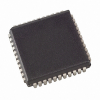
AT27C4096-55JU Atmel, AT27C4096-55JU Datasheet - Page 8

AT27C4096-55JU
Manufacturer Part Number
AT27C4096-55JU
Description
IC OTP 4MBIT 55NS 44PLCC
Manufacturer
Atmel
Specifications of AT27C4096-55JU
Format - Memory
EPROMs
Memory Type
OTP EPROM
Memory Size
4M (256K x 16)
Speed
55ns
Interface
Parallel
Voltage - Supply
4.5 V ~ 5.5 V
Operating Temperature
-40°C ~ 85°C
Package / Case
44-PLCC
Organization
512 K x 8
Access Time
55 ns
Supply Voltage (max)
5.5 V
Supply Voltage (min)
4.5 V
Maximum Operating Temperature
85 C
Interface Type
Parallel
Minimum Operating Temperature
- 40 C
Mounting Style
SMD/SMT
Capacitance, Input
4 pF
Capacitance, Output
8 pF
Current, Input, Leakage
±1 μA
Current, Operating
40 mA (Read)
Current, Output, Leakage
±5
Density
4M
Package Type
PLCC
Temperature, Operating
-40 to +85 °C
Time, Access
55 ns
Time, Address Setup
2
Time, Fall
20 ns
Time, Rise
20 ns
Voltage, Esd
2000 V
Voltage, Input, High
5.5 V (Read)
Voltage, Input, Low
0.8 V (Read)
Voltage, Output, High
2.4 V (Read)
Voltage, Output, Low
0.4 V (Read)
Voltage, Supply
5 V
Memory Configuration
256K X 16
Supply Voltage Range
4.5V To 5.5V
Memory Case Style
PLCC
No. Of Pins
44
Operating Temperature Range
-40°C To
Rohs Compliant
Yes
Lead Free Status / RoHS Status
Lead free / RoHS Compliant
Available stocks
Company
Part Number
Manufacturer
Quantity
Price
Company:
Part Number:
AT27C4096-55JU
Manufacturer:
ATMEL
Quantity:
2 185
Company:
Part Number:
AT27C4096-55JU
Manufacturer:
ATMEL
Quantity:
562
15. DC Programming Characteristics
T
16. AC Programming Characteristics
T
Notes:
17. Atmel’s AT27C4096 Intergrated Product Identification Code
8
A
Symbol
I
V
V
V
V
I
I
V
A
Symbol
t
t
t
t
t
t
t
t
t
t
t
Codes
Manufacturer
Device Type
LI
CC2
PP2
AS
OES
DS
AH
DH
DFP
VPS
VCS
PW
OE
PRT
OL
OH
IL
IH
ID
= 25 ± 5°C, V
= 25 ± 5°C, V
1. V
2. This parameter is only sampled and is not 100% tested. Output Float is defined as the point where data is no longer
3. Program Pulse width tolerance is 50 µsec ± 5%.
AT27C4096
driven – see timing diagram.
CC
Parameter
Input Load Current
Input Low Level
Input High Level
Output Low Voltage
Output High Voltage
V
V
A9 Product Identification Voltage
Parameter
Address Setup Time
OE Setup Time
Data Setup Time
Address Hold Time
Data Hold Time
OE High to Output Float Delay
V
V
CE Program Pulse Width
Data Valid from OE
V
Programming
CC
PP
PP
CC
PP
must be applied simultaneously or before V
CC
CC
Supply Current
Setup Time
Pulse Rise Time During
Supply Current (Program and Verify)
Setup Time
= 6.5 ± 0.25V, V
= 6.5 ± 0.25V, V
A0
0
1
O15-O8
PP
(3)
PP
0
0
= 13.0 ± 0.25V
= 13.0 ± 0.25V
(2)
O7
0
1
Test Conditions
Input Rise and Fall Times :
Input Pulse Levels:
Input Timing Reference Level:
Output Timing Reference Level:
PP
O6
Test Conditions
V
I
I
CE = V
0
1
OL
OH
IN
and removed simultaneously or after V
= 2.1 mA
= V
= -400 µA
IL
IL
(10% to 90%) 20 ns
, V
O5
0
1
(1)
IH
Pins
0.45V to 2.4V
0.8V to 2.0V
0.8V to 2.0V
O4
1
1
O3
1
0
11.5
Min
-0.6
47.5
Min
2.0
2.4
50
2
2
2
0
2
0
2
2
O2
1
1
PP
Limits
Limits
.
O1
1
0
V
CC
Max
12.5
Max
52.5
±10
130
150
0.8
0.4
50
30
+
0.7
O0
0
0
0311I–EPROM–12/07
Hex Data
Units
Units
mA
mA
001E
00F4
µA
µs
µs
µs
µs
µs
ns
µs
µs
µs
ns
ns
V
V
V
V
V


