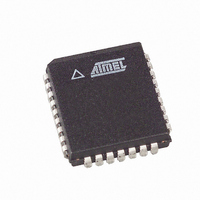
AT27LV010A-70JU Atmel, AT27LV010A-70JU Datasheet - Page 9

AT27LV010A-70JU
Manufacturer Part Number
AT27LV010A-70JU
Description
IC OTP 1MBIT 70NS 32PLCC
Manufacturer
Atmel
Datasheet
1.AT27LV010A-90JI.pdf
(15 pages)
Specifications of AT27LV010A-70JU
Format - Memory
EPROMs
Memory Type
OTP EPROM
Memory Size
1M (128K x 8)
Speed
70ns
Interface
Parallel
Voltage - Supply
3 V ~ 3.6 V, 4.5 V ~ 5.5 V
Operating Temperature
-40°C ~ 85°C
Package / Case
32-PLCC
Package
32PLCC
Density
1 Mb
Organization
128Kx8
Operating Supply Voltage
3.3|5 V
Maximum Random Access Time
70 ns
In System Programmability
External
Reprogramming Technique
OTP
Access Time
70 ns
Supply Voltage (max)
3.6 V or 5.5 V
Supply Voltage (min)
3 V or 4.5 V
Maximum Operating Temperature
85 C
Interface Type
Parallel
Minimum Operating Temperature
- 40 C
Mounting Style
SMD/SMT
Bus Type
Parallel
In System Programmable
External
Access Time (max)
70ns
Package Type
PLCC
Operating Supply Voltage (typ)
3.3/5V
Operating Supply Voltage (min)
3/4.5V
Operating Supply Voltage (max)
3.6/5.5V
Supply Current
8mA
Pin Count
32
Mounting
Surface Mount
Operating Temp Range
-40C to 85C
Operating Temperature Classification
Industrial
Lead Free Status / RoHS Status
Lead free / RoHS Compliant
Available stocks
Company
Part Number
Manufacturer
Quantity
Price
15. DC Programming Characteristics
T
16. AC Programming Characteristics
T
Notes:
17. Atmel’s AT27LV010A Integrated Product Identification Code
Note:
0548E–EPROM–12/07
Symbol
I
V
V
V
V
I
I
V
Symbol
t
t
t
t
t
t
t
t
t
t
t
t
A
A
Codes
Manufacturer
Device Type
LI
CC2
PP2
AS
CES
OES
DS
AH
DH
DFP
VPS
VCS
PW
OE
PRT
IL
IH
OL
OH
ID
= 25 ± 5°C, V
= 25 ± 5°C, V
1. V
2. This parameter is only sampled and is not 100% tested. Output Float is defined as the point where data is no longer driven –
3. Program Pulse width tolerance is 100 µsec ± 5%.
1. The AT27LV010A has the same Product Identification Code as the AT27C010. Both are programming compatible.
see timing diagram.
CC
Parameter
Input Load Current
Input Low Level
Input High Level
Output Low Voltage
Output High Voltage
V
V
A9 Product Identification Voltage
Parameter
Address Setup Time
CE Setup Time
OE Setup Time
Data Setup Time
Address Hold Time
Data Hold Time
OE High to Output Float Delay
V
V
PGM Program Pulse Width
Data Valid from OE
V
Programming
CC
PP
PP
CC
PP
must be applied simultaneously or before V
CC
CC
Pulse Rise Time During
Supply Current
Setup Time
Supply Current (Program and Verify)
Setup Time
= 6.5 ± 0.25V, V
= 6.5 ± 0.25V, V
A0
0
1
PP
PP
= 13.0 ± 0.25V
= 13.0 ± 0.2V
(3)
O7
0
0
(2)
O6
0
0
Test Conditions
Input Rise and Fall Times:
Input Pulse Levels:
Input Timing Reference Level:
Output Timing Reference Level:
Test Conditions
V
I
I
CE = PGM = V
PP
OL
OH
IN
and removed simultaneously or after V
O5
= 2.1 mA
= -400 µA
= V
0
0
IL
, V
(10% to 90%) 20 ns
IH
(1)
Pins
O4
1
0
IL
0.45V to 2.4V
0.8V to 2.0V
0.8V to 2.0V
O3
1
0
O2
1
1
11.5
Min
-0.6
Min
2.0
2.4
95
50
2
2
2
2
0
2
0
2
2
PP
Limits
Limits
.
O1
(1)
1
0
AT27LV010A
V
CC
Max
12.5
Max
130
105
150
±10
0.8
0.4
40
20
+ 0.5
O0
0
1
Units
Units
Data
mA
mA
Hex
µA
µs
µs
µs
µs
µs
µs
ns
µs
µs
µs
ns
ns
V
V
V
V
V
1E
05
9


