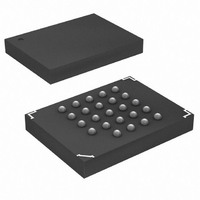
AT45DB321D-CU Atmel, AT45DB321D-CU Datasheet - Page 38

AT45DB321D-CU
Manufacturer Part Number
AT45DB321D-CU
Description
IC FLASH 32MBIT 66MHZ 24CBGA
Manufacturer
Atmel
Datasheet
1.AT45DB321D-MU.pdf
(57 pages)
Specifications of AT45DB321D-CU
Format - Memory
FLASH
Memory Type
DataFLASH
Memory Size
32M (8192 pages x 528 bytes)
Speed
66MHz
Interface
SPI, RapidS
Voltage - Supply
2.7 V ~ 3.6 V
Operating Temperature
-40°C ~ 85°C
Package / Case
24-CBGA
Lead Free Status / RoHS Status
Lead free / RoHS Compliant
Available stocks
Company
Part Number
Manufacturer
Quantity
Price
Company:
Part Number:
AT45DB321D-CU-SL383
Manufacturer:
Adesto Technologies
Quantity:
10 000
21.5
Figure 21-1. RapidS Mode
38
MOSI = Master Out, Slave In
MISO = Master In, Slave Out
The Master is the host controller and the Slave is the DataFlash
The Master always clocks data out on the rising edge of SCK and always clocks data in on the falling edge of SCK.
The Slave always clocks data out on the falling edge of SCK and always clocks data in on the rising edge of SCK.
Slave
Utilizing the RapidS
A.
B.
C.
D.
E.
F.
G. Master clocks in first bit of BYTE-SO.
H. Slave clocks out second bit of BYTE-SO.
I.
MOSI
MISO
AT45DB321D
SCK
Master clocks out first bit of BYTE-MOSI on the rising edge of SCK.
Slave clocks in first bit of BYTE-MOSI on the next rising edge of SCK.
Master clocks out second bit of BYTE-MOSI on the same rising edge of SCK.
Last bit of BYTE-MOSI is clocked out from the Master.
Last bit of BYTE-MOSI is clocked into the slave.
Slave clocks out first bit of BYTE-SO.
Master clocks in last bit of BYTE-SO.
CS
A
To take advantage of the RapidS function's ability to operate at higher clock frequencies, a full
clock cycle must be used to transmit data back and forth across the serial bus. The DataFlash is
designed to always clock its data out on the falling edge of the SCK signal and clock data in on
the rising edge of SCK.
For full clock cycle operation to be achieved, when the DataFlash is clocking data out on the fall-
ing edge of SCK, the host controller should wait until the next falling edge of SCK to latch the
data in. Similarly, the host controller should clock its data out on the rising edge of SCK in order
to give the DataFlash a full clock cycle to latch the incoming data in on the next rising edge of
SCK.
1
B
MSB
C
2
™
Function
3
4
BYTE-MOSI
5
6
7
D
8
E
LSB
F
1
G
MSB
2
H
3
4
BYTE-SO
5
6
7
8
3597O–DFLASH–10/09
I
LSB
1


