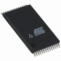
AT45DB321D-TU Atmel, AT45DB321D-TU Datasheet - Page 27

AT45DB321D-TU
Manufacturer Part Number
AT45DB321D-TU
Description
IC FLASH 32MBIT 66MHZ 28TSOP
Manufacturer
Atmel
Specifications of AT45DB321D-TU
Format - Memory
FLASH
Memory Type
DataFLASH
Memory Size
32M (8192 pages x 528 bytes)
Speed
66MHz
Interface
SPI, RapidS
Voltage - Supply
2.7 V ~ 3.6 V
Operating Temperature
-40°C ~ 85°C
Package / Case
28-TSOP
Architecture
Sectored
Interface Type
SPI
Supply Voltage (max)
3.6 V
Supply Voltage (min)
2.7 V
Maximum Operating Current
15 mA
Mounting Style
SMD/SMT
Organization
528 B x 8192
Memory Configuration
8192 Pages X 528 Bytes
Clock Frequency
20MHz
Supply Voltage Range
2.7V To 3.6V
Memory Case Style
TSOP
Rohs Compliant
Yes
Lead Free Status / RoHS Status
Lead free / RoHS Compliant
Available stocks
Company
Part Number
Manufacturer
Quantity
Price
Part Number:
AT45DB321D-TU
Manufacturer:
ATMEL/爱特梅尔
Quantity:
20 000
14.2
3597H–DFLASH–02/07
Operation Mode Summary
The commands described previously can be grouped into four different categories to better
describe which commands can be executed at what times.
Group A commands consist of:
Group B commands consist of:
Group C commands consist of:
Group D commands consist of:
If a Group A command is in progress (not fully completed), then another command in Group A,
B, C, or D should not be started. However, during the internally self-timed portion of Group B
commands, any command in Group C can be executed. The Group B commands using buffer 1
should use Group C commands using buffer 2 and vice versa. Finally, during the internally self-
timed portion of a Group D command, only the Status Register Read command should be
executed.
1. Main Memory Page Read
2. Continuous Array Read
3. Read Sector Protection Register
4. Read Sector Lockdown Register
5. Read Security Register
1. Page Erase
2. Block Erase
3. Sector Erase
4. Chip Erase
5. Main Memory Page to Buffer 1 (or 2) Transfer
6. Main Memory Page to Buffer 1 (or 2) Compare
7. Buffer 1 (or 2) to Main Memory Page Program with Built-in Erase
8. Buffer 1 (or 2) to Main Memory Page Program without Built-in Erase
9. Main Memory Page Program through Buffer 1 (or 2)
10. Auto Page Rewrite
1. Buffer 1 (or 2) Read
2. Buffer 1 (or 2) Write
3. Status Register Read
4. Manufacturer and Device ID Read
1. Erase Sector Protection Register
2. Program Sector Protection Register
3. Sector Lockdown
4. Program Security Register
AT45DB321D [Preliminary]
27


