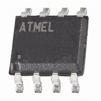
AT25DF021-SSH-T Atmel, AT25DF021-SSH-T Datasheet - Page 17

AT25DF021-SSH-T
Manufacturer Part Number
AT25DF021-SSH-T
Description
IC FLASH 2MBIT 70MHZ 8SOIC
Manufacturer
Atmel
Datasheet
1.AT25DF021-SSH-B.pdf
(41 pages)
Specifications of AT25DF021-SSH-T
Format - Memory
FLASH
Memory Type
DataFLASH
Memory Size
2M (256K x 8)
Speed
70MHz
Interface
SPI, 3-Wire Serial
Voltage - Supply
2.7 V ~ 3.6 V
Operating Temperature
-40°C ~ 85°C
Package / Case
8-SOIC (3.9mm Width)
Lead Free Status / RoHS Status
Lead free / RoHS Compliant
Available stocks
Company
Part Number
Manufacturer
Quantity
Price
Company:
Part Number:
AT25DF021-SSH-T
Manufacturer:
Atmel
Quantity:
4 000
9.6
3677D–DFLASH–04/09
Read Sector Protection Registers
SPRL bit from a logical “1” to a logical “0” provided the WP pin is deasserted. Likewise, the sys-
tem can write an F0h to change the SPRL bit from a logical “0” to a logical “1” without affecting
the current sector protection status (no changes will be made to the Sector Protection
Registers).
When writing to the first byte of the Status Register, bits 5, 4, 3, and 2 will not actually be modi-
fied but will be decoded by the device for the purposes of the Global Protect and Global
Unprotect functions. Only bit 7, the SPRL bit, will actually be modified. Therefore, when reading
the first byte of the Status Register, bits 5, 4, 3, and 2 will not reflect the values written to them
but will instead indicate the status of the WP pin and the sector protection status. Please refer to
“Read Status Register” on page 22
format and what values can be read for bits 5, 4, 3, and 2.
The Sector Protection Registers can be read to determine the current software protection status
of each sector. Reading the Sector Protection Registers, however, will not determine the status
of the WP pin.
To read the Sector Protection Register for a particular sector, the CS pin must first be asserted
and the opcode of 3Ch must be clocked in. Once the opcode has been clocked in, three address
bytes designating any address within the sector must be clocked in. After the last address byte
has been clocked in, the device will begin outputting data on the SO pin during every subse-
quent clock cycle. The data being output will be a repeating byte of either FFh or 00h to denote
the value of the appropriate Sector Protection Register.
Table 9-3.
Deasserting the CS pin will terminate the read operation and put the SO pin into a high-imped-
ance state. The CS pin can be deasserted at any time and does not require that a full byte of
data be read.
In addition to reading the individual Sector Protection Registers, the Software Protection Status
(SWP) bits in the Status Register can be read to determine if all, some, or none of the sectors
are software protected (refer to
Figure 9-5.
SCK
SO
CS
Output Data
SI
FFh
00h
Read Sector Protection Register - Output Data
Read Sector Protection Register
MSB
HIGH-IMPEDANCE
0
0
Sector Protection Register Value
Sector Protection Register value is 0 (sector is unprotected).
Sector Protection Register value is 1 (sector is protected).
0
1
1
2
OPCODE
1
3
1
4
1
5
“Read Status Register” on page 22
0
6
0
7
and
MSB
A
8
A
Table 11-1 on page 22
9
ADDRESS BITS A23-A0
A
10 11
A
A
12
A
A
29 30
A
A
31 32
MSB
for details on the Status Register
D
D
33
for more details).
DATA BYTE
D
34
D
35
D
36
D
37 38
D
D
39 40
MSB
D
D
17


