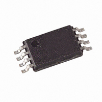
AT25080B-XHL-B Atmel, AT25080B-XHL-B Datasheet - Page 8

AT25080B-XHL-B
Manufacturer Part Number
AT25080B-XHL-B
Description
IC EEPROM 8KBIT 20MHZ 8TSSOP
Manufacturer
Atmel
Datasheet
1.AT25080B-PU.pdf
(26 pages)
Specifications of AT25080B-XHL-B
Format - Memory
EEPROMs - Serial
Memory Type
EEPROM
Memory Size
8K (1K x 8)
Speed
5MHz, 10MHz, 20MHz
Interface
SPI, 3-Wire Serial
Voltage - Supply
1.8 V ~ 5.5 V
Operating Temperature
-40°C ~ 85°C
Package / Case
8-TSSOP
Lead Free Status / RoHS Status
Lead free / RoHS Compliant
8
WRITE STATUS REGISTER (WRSR): The WRSR instruction allows the user to select one of four levels of protec-
tion. The AT25080B/160B is divided into four array segments. One-quarter, one-half, or all of the memory
segments can be protected. Any of the data within any selected segment will therefore be read only. The block
write protection levels and corresponding status register control bits are shown in
The three bits BP0, BP1, and WPEN are nonvolatile cells that have the same properties and functions as the regu-
lar memory cells (e.g., WREN, t
Table 3-4.
The WRSR instruction also allows the user to enable or disable the write protect (WP) pin through the use of the
Write Protect Enable (WPEN) bit. Hardware write protection is enabled when the WP pin is low and the WPEN bit
is “1”. Hardware write protection is disabled when either the WP pin is high or the WPEN bit is “0”. When the device
is hardware write protected, writes to the status register, including the block protect bits and the WPEN bit, and the
block-protected sections in the memory array are disabled. Writes are only allowed to sections of the memory that
are not block-protected.
Note:
Table 3-5.
READ SEQUENCE (READ): Reading the AT25080B/160B via the Serial Output (SO) pin requires the following
sequence. After the CS line is pulled low to select a device, the read op-code is transmitted via the SI line followed
by the byte address to be read (A15
The data (D7
line should be driven high after the data comes out. The read sequence can be continued since the byte address is
automatically incremented and data will continue to be shifted out. When the highest address is reached, the
address counter will roll over to the lowest address allowing the entire memory to be read in one continuous read
cycle.
Level
AT25080B/160B
WPEN
1(1/4)
2(1/2)
3(All)
0
0
1
1
X
X
0
When the WPEN bit is hardware write protected, it cannot be changed back to “0” as long as the WP pin is held low.
–
D0) at the specified address is then shifted out onto the SO line. If only one byte is to be read, the CS
Block Write Protect Bits
WPEN Operation
High
High
Low
Low
WP
X
X
Status Register Bits
BP1
0
0
1
1
WEN
0
1
0
1
0
1
WC
, RDSR).
–
A0, see
BP0
0
1
0
1
Protected
Protected
Protected
Protected
Protected
Protected
Protected
Blocks
Table
3-6). Upon completion, any data on the SI line will be ignored.
030003FF
020003FF
000003FF
AT25080B
None
Array Addresses Protected
Unprotected
Protected
Protected
Protected
Writeable
Writeable
Writeable
Blocks
060007FF
040007FF
000007FF
AT25160B
None
Protected
Writeable
Protected
Protected
Protected
Writeable
Register
Table
Status
3-4.
5228D–SEEPR–4/10


