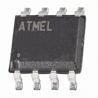
AT24HC02BN-SH-T Atmel, AT24HC02BN-SH-T Datasheet - Page 10

AT24HC02BN-SH-T
Manufacturer Part Number
AT24HC02BN-SH-T
Description
IC EEPROM 2KBIT 1MHZ 8SOIC
Manufacturer
Atmel
Specifications of AT24HC02BN-SH-T
Format - Memory
EEPROMs - Serial
Memory Type
EEPROM
Memory Size
2K (256 x 8)
Speed
400kHz, 1MHz
Interface
I²C, 2-Wire Serial
Voltage - Supply
1.8 V ~ 5.5 V
Operating Temperature
-40°C ~ 85°C
Package / Case
8-SOIC (3.9mm Width)
Density
2Kb
Interface Type
Serial (2-Wire)
Organization
256x8
Access Time (max)
900ns
Frequency (max)
400KHz
Write Protection
Yes
Data Retention
100Year
Operating Supply Voltage (typ)
2.5/3.3/5V
Package Type
SOIC
Operating Temp Range
-40C to 85C
Supply Current
3mA
Operating Supply Voltage (min)
1.8V
Operating Supply Voltage (max)
5.5V
Operating Temperature Classification
Industrial
Mounting
Surface Mount
Pin Count
8
Lead Free Status / RoHS Status
Lead free / RoHS Compliant
Other names
AT24HC02BN-10SU-1.8 SL383
AT24HC02BN-10SU-1.8 SL383
AT24HC02BN-10SU-1.8 SL383
Available stocks
Company
Part Number
Manufacturer
Quantity
Price
Part Number:
AT24HC02BN-SH-T
Manufacturer:
ATMEL/爱特梅尔
Quantity:
20 000
10. Read Operations
Figure 10-2. Byte Write
10
AT24HC02B/04B
Read operations are initiated the same way as write operations with the exception that the
read/write select bit in the device address word is set to “1”. There are three read operations:
current address read, random address read and sequential read.
CURRENT ADDRESS READ: The internal data word address counter maintains the last
address accessed during the last read or write operation, incremented by one. This address
stays valid between operations as long as the chip power is maintained. The address “roll over”
during read is from the last byte of the last memory page to the first byte of the first page. The
address “roll over” during write is from the last byte of the current page to the first byte of the
same page.
Once the device address with the read/write select bit set to “1” is clocked in and acknowledged
by the EEPROM, the current address data word is serially clocked out. The microcontroller does
not respond with an input “0” but does generate a following stop condition (see
page
RANDOM READ: A random read requires a “dummy” byte write sequence to load in the data
word address. Once the device address word and data word address are clocked in and
acknowledged by the EEPROM, the microcontroller must generate another start condition. The
microcontroller now initiates a current address read by sending a device address with the
read/write select bit high. The EEPROM acknowledges the device address and serially clocks
out the data word. The microcontroller does not respond with a “0” but does generate a following
stop condition (see
SEQUENTIAL READ: Sequential reads are initiated by either a current address read or a ran-
dom address read. After the microcontroller receives a data word, it responds with an
acknowledge. As long as the EEPROM receives an acknowledge, it will continue to increment
the data word address and serially clock out sequential data words. When the memory address
limit is reached, the data word address will “roll over” and the sequential read will continue. The
sequential read operation is terminated when the microcontroller does not respond with a “0” but
does generate a following stop condition (see
Figure 10-1. Device Address
11).
Figure 10-4 on page
2K
4K
MSB
MSB
1
1
0
0
11).
1
1
Figure 10-6 on page
0
0
A
A
A
A
A
P
R/W
LSB
R/W
LSB
11).
5192C–SEEPR–01/09
Figure 10-5 on


