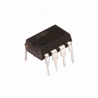
AT24HC02B-PU Atmel, AT24HC02B-PU Datasheet

AT24HC02B-PU
Specifications of AT24HC02B-PU
AT24HC02B-10PU-1.8
Available stocks
Related parts for AT24HC02B-PU
AT24HC02B-PU Summary of contents
Page 1
... Die Sales: Wafer Form, Tape and Reel, and Bumped Wafers Description The AT24HC02B provides 2048 bits of serial electrically erasable and programmable read-only memory (EEPROM) organized as 256 words of 8 bits each. The device is opti- mized for use in many industrial and commercial applications where low-power and low- voltage operation are essential ...
Page 2
... DEVICE/PAGE ADDRESSES (A2, A1, A0): The A2, A1 and A0 pins are device address inputs that must be hardwired for the AT24HC02B. As many as eight 2K devices may be addressed on a single bus system. (Device addressing is discussed in detail under Device Addressing, page 8). ...
Page 3
... Input/Output Capacitance (SDA) I/O C Input Capacitance (A IN Note: 1. This parameter is characterized and is not 100% tested. 5134D–SEEPR–4/07 AT24HC02B, 2K SERIAL EEPROM: The 2K is internally organized with 32 pages of 8 bytes each. Random word addressing requires an 8-bit data word address. = 25° 1.0 MHz SCL) 0 ...
Page 4
... Output Low Level V = 3.0V OL2 CC V Output Low Level V = 1.8V OL1 CC Note min and V max are reference only and are not tested AT24HC02B [Preliminary −40°C to +85° Test Condition Min 1.8 2.5 2.7 4.5 READ at 100 kHz WRITE at 100 kHz ...
Page 5
Table 5. AC Characteristics Applicable over recommended operating range from T 100 pF (unless otherwise noted) Symbol Parameter f Clock Frequency, SCL SCL t Clock Pulse Width Low LOW t Clock Pulse Width High HIGH t Noise Suppression Time I ...
Page 6
... The EEPROM sends a “0” to acknowledge that it has received each word. This happens during the ninth clock cycle. STANDBY MODE: The AT24HC02B features a low-power standby mode that is enabled: (a) upon power-up and (b) after the receipt of the Stop bit and the completion of any internal operations. ...
Page 7
Figure 4. Bus Timing 5134D–SEEPR–4/07 2-WIRE SOFTWARE RESET: After an interruption in protocol, power loss or system reset, any two-wire part can be reset by following these steps: (a) Clock cycles, (b) Look for SDA high in ...
Page 8
... The write cycle time t is the time from a valid stop condition of a write sequence to the end of the internal clear/write cycle. WR Figure 6. Output Acknowledge Device Addressing AT24HC02B [Preliminary] 8 ACK STOP CONDITION The 2K EEPROM device requires an 8-bit device address word following a start condi- tion to enable the chip for a read or write operation, as shown in Figure 7 ...
Page 9
... The data word address lower three (2K) bits are internally incremented following the receipt of each data word. The higher data word address bits are not incremented, retaining the memory page row location. When the word address, internally generated, reaches the page boundary, the following byte is placed at the beginning of the same page. If more than eight (2K) data words are transmitted to the EEPROM, the data word address will “ ...
Page 10
... Read Operations AT24HC02B [Preliminary] 10 ACKNOWLEDGE POLLING: Once the internally-timed write cycle has started and the EEPROM inputs are disabled, acknowledge polling can be initiated. This involves send- ing a start condition followed by the device address word. The read/write bit is representative of the operation desired. Only if the internal write cycle has completed will the EEPROM respond with a “ ...
Page 11
... As long as the EEPROM receives an acknowledge, it will continue to increment the data word address and serially clock out sequential data words. When the memory address limit is reached, the data word address will “roll over” and the sequen- tial read will continue. The sequential read operation is terminated when the microcontroller does not respond with a “ ...
Page 12
... AT24HC02B Ordering Information Ordering Code AT24HC02B-PU (Bulk form only) (1) AT24HC02BN-SH-B (NiPdAu Lead Finish) (2) AT24HC02BN-SH-T (NiPdAu Lead Finish) (1) AT24HC02B-TH-B (NiPdAu Lead Finish) (2) AT24HC02B-TH-T (NiPdAu Lead Finish) (3) AT24HC02B-W-11 Notes: 1. “-B” denotes bulk. 2. “-T” denotes tape and reel. SOIC = 4K per reel. TSSOP = 5K per reel. ...
Page 13
Packaging Information 8P3 – PDIP Top View PLCS Side View Notes: 1. This drawing is for general information only; refer to JEDEC Drawing MS-001, Variation BA, for additional information. 2. Dimensions A and L are measured ...
Page 14
... JEDEC SOIC Top View e Side View Note: These drawings are for general information only. Refer to JEDEC Drawing MS-012, Variation AA for proper dimensions, tolerances, datums, etc. 1150 E. Cheyenne Mtn. Blvd. Colorado Springs, CO 80906 R AT24HC02B [Preliminary TITLE 8S1, 8-lead (0.150" Wide Body), Plastic Gull Wing ...
Page 15
TSSOP Pin 1 indicator this corner N Top View Side View Notes: 1. This drawing is for general information only. Refer to JEDEC Drawing MO-153, Variation AA, for proper dimensions, tolerances, datums, ...
Page 16
... Revision History AT24HC02B [Preliminary] 16 Doc. Rev. Date Comments 5134D 4/2007 Removed reference to Waffle Pack on page 1 Added lines to Ordering Code table Shrink Pin Diagram; Change to Table 5; Added Two-Wire Software Reset; Removed LSB from figures 5134C 3/2007 Pg Change to new catalog part number scheme. ...
Page 17
... Disclaimer: The information in this document is provided in connection with Atmel products. No license, express or implied, by estoppel or otherwise, to any intellectual property right is granted by this document or in connection with the sale of Atmel products. EXCEPT AS SET FORTH IN ATMEL’S TERMS AND CONDI- TIONS OF SALE LOCATED ON ATMEL’S WEB SITE, ATMEL ASSUMES NO LIABILITY WHATSOEVER AND DISCLAIMS ANY EXPRESS, IMPLIED OR STATUTORY WARRANTY RELATING TO ITS PRODUCTS INCLUDING, BUT NOT LIMITED TO, THE IMPLIED WARRANTY OF MERCHANTABILITY, FITNESS FOR A PARTICULAR PURPOSE, OR NON-INFRINGEMENT ...


