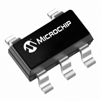
24LC00T/OT Microchip Technology, 24LC00T/OT Datasheet - Page 6

24LC00T/OT
Manufacturer Part Number
24LC00T/OT
Description
IC EEPROM 128BIT 400KHZ SOT23-5
Manufacturer
Microchip Technology
Datasheet
1.24C00T-IOT.pdf
(24 pages)
Specifications of 24LC00T/OT
Memory Size
128 (16 x 8)
Format - Memory
EEPROMs - Serial
Memory Type
EEPROM
Speed
100kHz, 400kHz
Interface
I²C, 2-Wire Serial
Voltage - Supply
2.5 V ~ 5.5 V
Operating Temperature
0°C ~ 70°C
Package / Case
SOT-23-5, SC-74A, SOT-25
Memory Configuration
16 X 8
Ic Interface Type
I2C
Clock Frequency
400MHz
Supply Voltage Range
2.5V To 5.5V
Memory Case Style
SOT-23
No. Of Pins
5
Lead Free Status / RoHS Status
Lead free / RoHS Compliant
Other names
24LC00/OT
24LC00/OT
Q636229
24LC00/OT
Q636229
Available stocks
Company
Part Number
Manufacturer
Quantity
Price
Company:
Part Number:
24LC00T/OT
Manufacturer:
MICROCHIP
Quantity:
12 000
Part Number:
24LC00T/OT
Manufacturer:
MICROCHIP/微芯
Quantity:
20 000
24AA00/24LC00/24C00
5.0
After generating a Start condition, the bus master
transmits a control byte consisting of a slave address
and a Read/Write bit that indicates what type of
operation is to be performed. The slave address for the
24XX00 consists of a 4-bit device code ‘1010’ followed
by three “don’t care” bits.
The last bit of the control byte determines the operation
to be performed. When set to a one a read operation is
selected, and when set to a zero a write operation is
selected (Figure 5-1). The 24XX00 monitors the bus for
its corresponding slave address all the time. It
generates an Acknowledge bit if the slave address was
true and it is not in a programming mode.
FIGURE 5-1:
DS21178G-page 6
Start Bit
S
DEVICE ADDRESSING
1
Device Select
0
Bits
Slave Address
1
CONTROL BYTE FORMAT
0
Read/Write Bit
Don’t Care
x
Acknowledge Bit
Bits
x
x
R/W
ACK
6.0
6.1
Following the Start signal from the master, the device
code (4 bits), the “don’t care” bits (3 bits), and the R/W
bit (which is a logic low) are placed onto the bus by the
master transmitter. This indicates to the addressed
slave receiver that a byte with a word address will
follow after it has generated an Acknowledge bit during
the ninth clock cycle. Therefore, the next byte transmit-
ted by the master is the word address and will be
written into the Address Pointer of the 24XX00. Only
the lower four address bits are used by the device, and
the upper four bits are “don’t cares.” The 24XX00 will
acknowledge the address byte and the master device
will then transmit the data word to be written into the
addressed memory location. The 24XX00 acknowl-
edges again and the master generates a Stop
condition. This initiates the internal write cycle, and
during this time the 24XX00 will not generate Acknowl-
edge signals (Figure 7-2). After a byte Write command,
the internal address counter will not be incremented
and will point to the same address location that was just
written. If a Stop bit is transmitted to the device at any
point in the Write command sequence before the entire
sequence is complete, then the command will abort
and no data will be written. If more than 8 data bits are
transmitted before the Stop bit is sent, then the device
will clear the previously loaded byte and begin loading
the data buffer again. If more than one data byte is
transmitted to the device and a Stop bit is sent before a
full eight data bits have been transmitted, then the
Write command will abort and no data will be written.
The 24XX00 employs a V
which disables the internal erase/write logic if the V
is below 1.5V (24AA00 and 24LC00) or 3.8V (24C00)
at nominal conditions.
WRITE OPERATIONS
Byte Write
© 2007 Microchip Technology Inc.
CC
threshold detector circuit
CC


