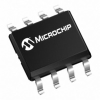
93AA46C-I/MS Microchip Technology, 93AA46C-I/MS Datasheet - Page 7

93AA46C-I/MS
Manufacturer Part Number
93AA46C-I/MS
Description
IC EEPROM 1KBIT 3MHZ 8MSOP
Manufacturer
Microchip Technology
Specifications of 93AA46C-I/MS
Memory Size
1K (128 x 8 or 64 x 16)
Package / Case
8-MSOP, Micro8™, 8-uMAX, 8-uSOP,
Operating Temperature
-40°C ~ 85°C
Format - Memory
EEPROMs - Serial
Memory Type
EEPROM
Speed
3MHz
Interface
Microwire, 3-Wire Serial
Voltage - Supply
1.8 V ~ 5.5 V
Organization
64 x 16 or 128 K x 8
Interface Type
Microwire
Maximum Clock Frequency
1 MHz
Supply Voltage (max)
5.5 V
Supply Voltage (min)
1.8 V
Maximum Operating Current
2 mA
Maximum Operating Temperature
+ 85 C
Mounting Style
SMD/SMT
Minimum Operating Temperature
- 40 C
Operating Supply Voltage
5.5 V
Memory Configuration
128 X 8, 64 X 16
Clock Frequency
3MHz
Supply Voltage Range
1.8V To 5.5V
Memory Case Style
MSOP
No. Of Pins
8
Rohs Compliant
Yes
Lead Free Status / RoHS Status
Lead free / RoHS Compliant
Lead Free Status / RoHS Status
Lead free / RoHS Compliant, Lead free / RoHS Compliant
Available stocks
Company
Part Number
Manufacturer
Quantity
Price
Part Number:
93AA46C-I/MS
Manufacturer:
MICROCHIP/微芯
Quantity:
20 000
2.4
The ERASE instruction forces all data bits of the
specified address to the logical ‘1’ state. CS is brought
low following the loading of the last address bit. This
falling edge of the CS pin initiates the self-timed
programming cycle, except on ‘93C’ devices where the
rising edge of CLK before the last address bit initiates
the write cycle.
FIGURE 2-1:
FIGURE 2-2:
© 2005 Microchip Technology Inc.
CLK
CLK
DO
DO
CS
DI
CS
DI
Erase
93AA46A/B/C, 93LC46A/B/C, 93C46A/B/C
High-Z
High-Z
1
1
ERASE TIMING FOR 93AA AND 93LC DEVICES
ERASE TIMING FOR 93C DEVICES
1
1
1
1
A
A
N
N
A
A
N
N
-1 A
-1 A
N
N
-2
-2
•••
•••
The DO pin indicates the Ready/Busy status of the
device if CS is brought high after a minimum of 250 ns
low (T
is still in progress. DO at logical ‘1’ indicates that the
register at the specified address has been erased and
the device is ready for another instruction.
A0
A0
Note:
T
T
CSL
CSL
CSL
). DO at logical ‘0’ indicates that programming
After the Erase cycle is complete, issuing
a Start bit and then taking CS low will clear
the Ready/Busy status from DO.
T
WC
T
T
T
SV
WC
SV
Check Status
Check Status
Busy
Busy
Ready
Ready
DS21749F-page 7
High-Z
High-Z
T
T
CZ
CZ


