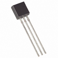
DS2502-E48+ Maxim Integrated Products, DS2502-E48+ Datasheet - Page 5

DS2502-E48+
Manufacturer Part Number
DS2502-E48+
Description
IC OTP 1KBIT TO92-3
Manufacturer
Maxim Integrated Products
Specifications of DS2502-E48+
Format - Memory
EPROMs (with MAC Address)
Memory Type
OTP EPROM
Memory Size
1K (1K x 1)
Interface
1-Wire Serial
Operating Temperature
-40°C ~ 85°C
Package / Case
TO-92-3 (Standard Body), TO-226
Organization
1 K x 1
Supply Voltage (max)
6 V
Supply Voltage (min)
2.8 V
Maximum Operating Temperature
+ 85 C
Minimum Operating Temperature
- 40 C
Mounting Style
Through Hole
Lead Free Status / RoHS Status
Lead free / RoHS Compliant
Voltage - Supply
-
Speed
-
Lead Free Status / Rohs Status
Lead free / RoHS Compliant
DS2502
1024-BITS EPROM
The memory map in Figure 5 shows the 1024-bit EPROM section of the DS2502 which is configured as
four pages of 32 bytes each. The 8-bit scratchpad is an additional register that acts as a buffer when
programming the memory. Data is first written to the scratchpad and then verified by reading an 8-bit
CRC from the DS2502 that confirms proper receipt of the data. If the buffer contents are correct, a
programming voltage should be applied and the byte of data will be written into the selected address in
memory. This process ensures data integrity when programming the memory. The details for reading and
programming the 1024-bit EPROM portion of the DS2502 are given in the Memory Function Commands
section.
EPROM STATUS BYTES
In addition to the 1024 bits of data memory the DS2502 provides 64 bits of Status Memory accessible
with separate commands.
The EPROM Status Bytes can be read or programmed to indicate various conditions to the software
interrogating the DS2502. The first byte of the EPROM Status Memory contain the Write Protect Page
bits which inhibit programming of the corresponding page in the 1024-bit main memory area if the
appropriate write protection bit is programmed. Once a bit has been programmed in the Write Protect
Page byte, the entire 32-byte page that corresponds to that bit can no longer be altered but may still be
read.
The next 4 bytes of the EPROM Status Memory contain the Page Address Redirection Bytes, which
indicate if one or more of the pages of data in the 1026-bit EPROM section have been invalidated and
redirected to the page address contained in the appropriate redirection byte. The hardware of the DS2502
makes no decisions based on the contents of the Page Address Redirection Bytes. These additional bytes
of Status EPROM technology, bits within a page can be changed from a logical 1 to a logical 0 by
programming, but cannot be changed back. Therefore, it is not possible to simply rewrite a page if the
data requires changing or updating, but with space permitting, an entire page of data can be redirected to
another page within the DS2502 by writing the one’s complement of the new page address into the Page
Address Redirection Byte that corresponds to the original (replaced) page.
This architecture allows the user’s software to make a “data patch” to the EPROM by indicating that a
particular page or pages should be replaced with those indicated in the Page Address Redirection Bytes.
If a Page Address Redirection Byte has an FFH value, the data in the main memory that corresponds to
that page is valid. If a Page Address Redirection Byte has some other hex value, the data in the page
corresponding to that redirection byte is invalid, and the valid data can now be found at the one’s
complement of the page address indicated by the hex value stored in the associated Page Address
Redirection Byte. A value of FDH in the redirection byte for page 1, for example, would indicate that the
updated data is now in page 2. The details for reading and programming the EPROM status memory
portion of the DS2502 are given in the Memory Function Commands section.
MEMORY FUNCTION COMMANDS
The “Memory Function Flow Chart” (Figure 6) describes the protocols necessary for accessing the
various data fields within the DS2502. The Memory Function Control section, 8-bit scratchpad, and the
Program Voltage Detect circuit combine to interpret the commands issued by the bus master and create
the correct control signals within the device. A 3-byte protocol is issued by the bus master. It is
comprised of a command byte to determine the type of operation and two address bytes to determine the
specific starting byte location within a data field. The command byte indicates if the device is to be read
5 of 23


