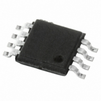
M93C46-WDW6TP STMicroelectronics, M93C46-WDW6TP Datasheet - Page 19

M93C46-WDW6TP
Manufacturer Part Number
M93C46-WDW6TP
Description
IC EEPROM 1KBIT 2MHZ 8TSSOP
Manufacturer
STMicroelectronics
Specifications of M93C46-WDW6TP
Format - Memory
EEPROMs - Serial
Memory Type
EEPROM
Memory Size
1K (128 x 8 or 64 x 16)
Speed
2MHz
Interface
Microwire, 3-Wire Serial
Voltage - Supply
2.5 V ~ 5.5 V
Operating Temperature
-40°C ~ 85°C
Package / Case
8-TSSOP
Organization
128 K x 8
Interface Type
Microwire
Maximum Clock Frequency
2 MHz
Supply Voltage (max)
5.5 V
Supply Voltage (min)
2.5 V
Maximum Operating Current
2 mA
Maximum Operating Temperature
+ 85 C
Mounting Style
SMD/SMT
Minimum Operating Temperature
- 40 C
Operating Supply Voltage
2.5 V, 5.5 V
Lead Free Status / RoHS Status
Lead free / RoHS Compliant
Other names
497-8655-2
M93C46-WDW6TP
M93C46-WDW6TP
Available stocks
Company
Part Number
Manufacturer
Quantity
Price
Company:
Part Number:
M93C46-WDW6TP
Manufacturer:
STMicroelectronics
Quantity:
28 615
Company:
Part Number:
M93C46-WDW6TP
Manufacturer:
SANYO
Quantity:
2 449
Part Number:
M93C46-WDW6TP
Manufacturer:
ST
Quantity:
20 000
M93C86, M93C76, M93C66, M93C56, M93C46
9
Clock pulse counter
In a noisy environment, the number of pulses received on Serial Clock (C) may be greater
than the number delivered by the master (the microcontroller). This can lead to a
misalignment of the instruction of one or more bits (as shown in
the writing of erroneous data at an erroneous address.
To combat this problem, the M93Cx6 has an on-chip counter that counts the clock pulses
from the start bit until the falling edge of the Chip Select Input (S). If the number of clock
pulses received is not the number expected, the WRITE, ERASE, ERAL or WRAL
instruction is aborted, and the contents of the memory are not modified.
The number of clock cycles expected for each instruction, and for each member of the
M93Cx6 family, are summarized in
Memory (WRITE) instruction on the M93C56 (or M93C66) expects 20 clock cycles (for the
x8 organization) from the start bit to the falling edge of Chip Select Input (S). That is:
Figure 7.
S
D
C
1 Start bit
+ 2 Op-code bits
+ 9 Address bits
+ 8 Data bits
START
Write sequence with one clock glitch
"0"
WRITE
Doc ID 4997 Rev 11
"1"
Table 5.
An
to
Glitch
Table
An-1
ARE SHIFTED BY ONE BIT
ADDRESS AND DATA
7.. For example, a Write Data to
An-2
Figure
Clock pulse counter
7.) and may lead to
D0
AI01395
19/36


