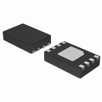
CAT34C02VP2I-GT4 ON Semiconductor, CAT34C02VP2I-GT4 Datasheet - Page 3

CAT34C02VP2I-GT4
Manufacturer Part Number
CAT34C02VP2I-GT4
Description
IC EEPROM 2KBIT 400KHZ 8TDFN
Manufacturer
ON Semiconductor
Specifications of CAT34C02VP2I-GT4
Format - Memory
EEPROMs - Serial
Memory Type
EEPROM
Memory Size
2K (256 x 8)
Speed
400kHz
Interface
I²C, 2-Wire Serial
Voltage - Supply
1.7 V ~ 5.5 V
Operating Temperature
-40°C ~ 85°C
Package / Case
8-VFDFN Exposed Pad
Density
2Kb
Interface Type
Serial (I2C)
Organization
256x8
Access Time (max)
900ns
Frequency (max)
400KHz
Write Protection
Yes
Data Retention
100Year
Operating Supply Voltage (typ)
1.8/2.5/3.3/5V
Operating Temp Range
-40C to 85C
Supply Current
2mA
Operating Supply Voltage (min)
1.7V
Operating Supply Voltage (max)
5.5V
Operating Temperature Classification
Industrial
Mounting
Surface Mount
Pin Count
8
Lead Free Status / RoHS Status
Lead free / RoHS Compliant
Other names
34C02VP2I-GT4
CAT34C02VP2I-GT4TR
CAT34C02VP2I-GT4TR
Available stocks
Company
Part Number
Manufacturer
Quantity
Price
Company:
Part Number:
CAT34C02VP2I-GT4
Manufacturer:
ON Semiconductor
Quantity:
83 445
Company:
Part Number:
CAT34C02VP2I-GT4
Manufacturer:
ON Semiconductor
Quantity:
3 000
Part Number:
CAT34C02VP2I-GT4
Manufacturer:
ON/安森美
Quantity:
20 000
6. Test conditions according to “A.C. Test Conditions” table.
7. Tested initially and after a design or process change that affects this parameter.
8. t
9. T
10. T
Table 5. A.C. CHARACTERISTICS
Table 6. THERMAL CHARACTERISTICS
Table 7. A.C. TEST CONDITIONS
CAT34C02Y
CAT34C02VP2
CAT34C02HU3
CAT34C02HU4
Input Levels
Input Rise and Fall Times
Input Reference Levels
Output Reference Levels
Output Load
t
Example: CAT34C02VP2, V
PU
PU
J
J
= T
= T
t
t
T
R
F
(Notes 7 & 8)
is the delay between the time V
Symbol
i
t
t
t
t
t
t
t
SU:STO
HD:STA
SU:STA
HD:DAT
SU:DAT
(Note 7)
(Note 7)
(Note 7)
HD:WP
t
SU:WP
F
t
A
t
C
HIGH
LOW
t
t
BUF
t
WR
SCL
AA
DH
+ P
+ P
D
D
* q
* q
Part Number
JA
JC
, where: T
, where: T
Clock Frequency
START Condition Hold Time
Low Period of SCL Clock
High Period of SCL Clock
START Condition Setup Time
Data Hold Time
Data Setup Time
SDA and SCL Rise Time
SDA and SCL Fall Time
STOP Condition Setup Time
Bus Free Time Between STOP and START
SCL Low to SDA Data Out
Data Out Hold Time
Noise Pulse Filtered at SCL and SDA Inputs
WP Setup Time
WP Hold Time
Write Cycle Time
Power−up to Ready Mode
CC
J
C
is the Junction Temperature, T
is the Case Temperature, etc.
= 3.0 V, I
CC
0.2 V
≤ 50 ns
0.3 V
0.5 V
Current Source: I
is stable and the device is ready to accept commands.
(V
CCmax
CC
CC
CC
CC
, 0.7 V
= 1.7 V to 5.5 V, T
to 0.8 V
(Air velocity = 0 m/s, 4 layers PCB) (Notes 9 and 10)
Parameter
= 1 mA, T
CC
CC
OL
http://onsemi.com
= 3 mA (V
A
= 85°C: T
Package
TSSOP
A
UDFN
UDFN
TDFN
the Ambient Temperature, P
A
= −40°C to +85°C) (Note 6)
3
CC
J
= 85°C + 3 mW * 92°C/W = 85.276°C.
≥ 2.5 V); I
OL
= 1 mA (V
Min
250
100
q
101
101
4.7
4.7
4.7
2.5
64
92
4
4
0
4
0
JA
D
Standard
the Power dissipation.
CC
< 2.5 V); C
1000
Max
100
300
100
3.5
5
1
L
Min
100
100
= 100 pF
0.6
1.3
0.6
0.6
0.6
1.3
2.5
0
0
q
37
15
18
18
Fast
JC
Max
400
300
300
100
0.9
5
1
Units
Units
°C/W
°C/W
°C/W
°C/W
kHz
ms
ms
ms
ms
ms
ms
ms
ns
ns
ns
ms
ms
ms
ns
ns
ms
ms


