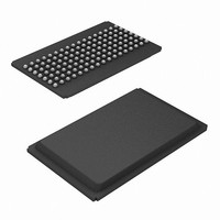
CY7C1370D-200BGXC Cypress Semiconductor Corp, CY7C1370D-200BGXC Datasheet - Page 9

CY7C1370D-200BGXC
Manufacturer Part Number
CY7C1370D-200BGXC
Description
IC SRAM 18MBIT 200MHZ 119BGA
Manufacturer
Cypress Semiconductor Corp
Type
Synchronousr
Specifications of CY7C1370D-200BGXC
Memory Size
18M (512K x 36)
Package / Case
119-BGA
Format - Memory
RAM
Memory Type
SRAM - Synchronous
Speed
200MHz
Interface
Parallel
Voltage - Supply
3.135 V ~ 3.6 V
Operating Temperature
0°C ~ 70°C
Access Time
3 ns
Maximum Clock Frequency
200 MHz
Supply Voltage (max)
3.6 V
Supply Voltage (min)
3.135 V
Maximum Operating Current
300 mA
Maximum Operating Temperature
+ 70 C
Minimum Operating Temperature
0 C
Mounting Style
SMD/SMT
Number Of Ports
4
Operating Supply Voltage
3.3 V
Lead Free Status / RoHS Status
Lead free / RoHS Compliant
Lead Free Status / RoHS Status
Lead free / RoHS Compliant, Lead free / RoHS Compliant
Available stocks
Company
Part Number
Manufacturer
Quantity
Price
Company:
Part Number:
CY7C1370D-200BGXC
Manufacturer:
Cypress Semiconductor Corp
Quantity:
10 000
Cycle Description table for details) inputs is latched into the
device and the write is complete.
The data written during the write operation is controlled by BW
(BW
The CY7C1370D/CY7C1372D provides byte write capability that
is described in the Write Cycle Description table. Asserting the
Write Enable input (WE) with the selected Byte Write Select
(BW) input will selectively write to only the desired bytes. Bytes
not selected during a byte write operation will remain unaltered.
A synchronous self-timed write mechanism has been provided
to simplify the write operations. Byte write capability has been
included in order to greatly simplify Read/Modify/Write
sequences, which can be reduced to simple byte write opera-
tions.
Because the CY7C1370D and CY7C1372D are common I/O
devices, data should not be driven into the device while the
outputs are active. The Output Enable (OE) can be deasserted
HIGH
(DQ
CY7C1372D) inputs. Doing so will tristate the output drivers. As
a safety precaution, DQ and DQP (DQ
CY7C1370D and DQ
cally tristated during the data portion of a write cycle, regardless
of the state of OE.
Burst Write Accesses
The CY7C1370D/CY7C1372D has an on-chip burst counter that
allows the user the ability to supply a single address and conduct
up to four write operations without reasserting the address
inputs. ADV/LD must be driven LOW in order to load the initial
address, as described in the Single Write Access section above.
When ADV/LD is driven HIGH on the subsequent clock rise, the
chip enables (CE
and the burst counter is incremented. The correct BW (BW
for CY7C1370D and BW
Table 3. ZZ Mode Electrical Characteristics
Document Number: 38-05555 Rev. *H
I
t
t
t
t
DDZZ
ZZS
ZZREC
ZZI
RZZI
a,b,c,d
a,b,c,d
Parameter
before
/DQP
for CY7C1370D and BW
a,b,c,d
presenting
1
, CE
a,b
Sleep mode standby current
Device operation to ZZ
ZZ recovery time
ZZ active to sleep current
ZZ Inactive to exit sleep current
for CY7C1370D and DQ
2
/DQP
, and CE
a,b
a,b
for CY7C1372D) inputs must be
data
for CY7C1372D) are automati-
3
Description
) and WE inputs are ignored
a,b
to
for CY7C1372D) signals.
the
a,b,c,d
DQ and
/DQP
a,b
/DQP
a,b,c,d
a,b
a,b,c,d
DQP
ZZ > V
ZZ > V
ZZ < 0.2V
This parameter is sampled
This parameter is sampled
for
for
DD
DD
driven in each cycle of the burst write in order to write the correct
bytes of data.
Sleep Mode
The ZZ input pin is an asynchronous input. Asserting ZZ places
the SRAM in a power conservation “sleep” mode. Two clock
cycles are required to enter into or exit from this “sleep” mode.
While in this mode, data integrity is guaranteed. Accesses
pending when entering the “sleep” mode are not considered valid
nor is the completion of the operation guaranteed. The device
must be deselected prior to entering the “sleep” mode. CE
and CE
ZZ input returns LOW.
Table 1. Interleaved Burst Address Table
(MODE = Floating or V
Table 2. Linear Burst Address Table (MODE = GND)
Test Conditions
− 0.2V
− 0.2V
Address
Address
A1,A0
First
A1,A0
First
00
01
10
11
00
01
10
11
3
, must remain inactive for the duration of t
Address
Second
A1,A0
Address
Second
CY7C1370D, CY7C1372D
A1,A0
01
10
11
00
01
00
11
10
DD
)
2t
Min.
CYC
0
Address
A1,A0
Third
Address
A1,A0
10
00
01
11
Third
10
00
01
11
2t
2t
Max.
80
CYC
CYC
ZZREC
Address
Address
Fourth
A1,A0
Fourth
Page 9 of 29
A1,A0
00
01
10
Unit
11
mA
11
10
01
00
ns
ns
ns
ns
after the
1
, CE
2
[+] Feedback
,


