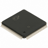
CY7C0241-15AXC Cypress Semiconductor Corp, CY7C0241-15AXC Datasheet

CY7C0241-15AXC
Specifications of CY7C0241-15AXC
Available stocks
Related parts for CY7C0241-15AXC
CY7C0241-15AXC Summary of contents
Page 1
... Features ■ True dual-ported memory cells, which allow simultaneous reads of the same memory location [1] ■ organization (CY7C024/024A ■ organization (CY7C0241) ■ organization (CY7C025) ■ organization (CY7C0251) ■ 0.65 micron CMOS for optimum speed and power ■ High speed access ■ Low operating power: I ...
Page 2
... Notes 2. BUSY is an output in master mode and an input in slave mode. 3. I/O –I/O on the CY7C0241/0251 I/O –I/O on the CY7C0241/0251 the CY7C025/0251. 12L the CY7C025/0251. 12R Document #: 38-06035 Rev. *D I/O I/O CONTROL CONTROL MEMORY ADDRESS ADDRESS ARRAY DECODER DECODER INTERRUPT CE CE ...
Page 3
Pin Configurations (continued) 100 I/O 10L 5 I/O 6 11L I/O 12L 7 I/O 13L 8 GND 9 I/O 10 14L I/O 11 15L GND ...
Page 4
... RAM cells, I/O and address lines, and control signals (CE, OE, R/W). These control pins permit independent access for reads or writes to any location in memory. To handle simultaneous writes/reads to the same location, a BUSY pin is provided on each port. Two interrupt (INT) pins can be used for port-to-port communication ...
Page 5
... HIGH during SEM LOW). A0–2 represents the semaphore address. OE and R/W are used in the same manner as a normal memory access. When writing or reading a semaphore, the other address pins have no effect. When writing to the semaphore, only I/O written to the left port of an available semaphore, a one appears at the same semaphore address on the right port ...
Page 6
Table 3. Semaphore Operation Example I/O 0 Function No action Left port writes 0 to semaphore Right port writes 0 to semaphore Left port writes 1 to semaphore Left port writes 0 to semaphore Right port writes 1 to semaphore ...
Page 7
Maximum Ratings [10] Exceeding maximum ratings may shorten the useful life of the device. User guidelines are not tested. Storage Temperature ................................. –65°C to +150°C Ambient Temperature with Power Applied ............................................ –55°C to +125°C Supply Voltage to Ground Potential................–0.3V to ...
Page 8
Electrical Characteristics Over the Operating Range (continued) Parameter Description I Operating Current V CC Outputs Disabled I Standby Current CE SB1 (Both Ports TTL Levels Standby Current CE SB2 (One Port TTL Level ...
Page 9
Switching Characteristics Over the Operating Range Parameter Description Read Cycle t Read Cycle Time RC t Address to Data Valid AA t Output Hold From Address OHA Change [15 LOW to Data Valid ACE t OE LOW to ...
Page 10
Switching Characteristics Over the Operating Range (continued) Parameter Description [20] Busy Timing t BUSY LOW from Address BLA Match t BUSY HIGH from Address BHA Mismatch t BUSY LOW from CE LOW BLC t BUSY HIGH from CE HIGH BHC ...
Page 11
Switching Waveforms Figure 4. Read Cycle No. 1 (Either Port Address Access) ADDRESS OHA DATA OUT PREVIOUS DATA VALID Figure 5. Read Cycle No. 2 (Either Port CE/OE Access) CE and DATA OUT ...
Page 12
Switching Waveforms (continued) Figure 7. Write Cycle No. 1: R/W Controlled Timing ADDRESS OE [32,33 R/W NOTE 35 DATA OUT DATA IN Figure 8. Write Cycle No Controlled Timing ADDRESS [32,33 R/W ...
Page 13
Switching Waveforms (continued) Figure 9. Semaphore Read After Write Timing, Either Side A –A VALID ADRESS SEM I R/W OE Figure 10. Timing Diagram of Semaphore Contention A – R/W L ...
Page 14
Switching Waveforms (continued) Figure 11. Timing Diagram of Read with BUSY (M/S=HIGH) ADDRESS R R/W R DATA ADDRESS L BUSY L DATA OUTL Figure 12. Write Timing with Busy Input (M/S=LOW) R/W BUSY Note 41. CE ...
Page 15
Switching Waveforms (continued) Figure 13. Busy Timing Diagram No.1 (CE Arbitration) CE Valid First: L ADDRESS L BUSY R CE Valid First: R ADDRESS L BUSY L Figure 14. Busy Timing Diagram ...
Page 16
Switching Waveforms (continued) Left Side Sets INT : R ADDRESS WRITE FFF (1FFF CY7C025 R/W L INT R [44] t INS Right Side Clears INT : R ADDRESS R INT R ...
Page 17
Ordering Information 4K x16 Dual-Port SRAM) ( Speed (ns) Ordering Code 15 CY7C024–15AC CY7C024-15AXC CY7C024–15JC CY7C024-15JXC 25 CY7C024–25AC CY7C024-25AXC CY7C024–25JC CY7C024A-25JXC CY7C024–25AI CY7C024-25AXI CY7C024–25JI CY7C024-25JXI 35 CY7C024–35AC CY7C024-35AXC CY7C024–35JC CY7C024-35JXC CY7C024–35AI CY7C024-35AXI CY7C024–35JI CY7C024-35JXI 55 CY7C024–55AC CY7C024-55AXC CY7C024–55JC CY7C024-55JXC CY7C024–55AI ...
Page 18
... CY7C025–55AC CY7C025-55AXC CY7C025–55JC CY7C025-55JXC CY7C025–55AI CY7C025-55AXI CY7C025–55JI CY7C025-55JXI Ordering Information ( Dual-Port SRAM) Speed (ns) Ordering Code 15 CY7C0241–15AC CY7C0241-15AXC CY7C0241–15AI CY7C0241-15AXI 25 CY7C0241–25AC CY7C0241-25AXC CY7C0241–25AI CY7C0241-25AXI 35 CY7C0241–35AC CY7C0241-35AXC CY7C0241–35AI CY7C0241-35AXI Document #: 38-06035 Rev. *D (continued) ...
Page 19
... Ordering Information ( Dual-Port SRAM) Speed (ns) Ordering Code 55 CY7C0241–55AC CY7C0241-55AXC CY7C0241–55AI CY7C0241-55AXI Dual-Port SRAM Speed (ns) Ordering Code 15 CY7C0251–15AC CY7C0251–15AXC 25 CY7C0251–25AC CY7C0251-25AXC CY7C0251–25AI CY7C0251–25AXI 35 CY7C0251–35AC CY7C0251–35AXC CY7C0251–35AI CY7C0251–35AXI 55 CY7C0251–55AC CY7C0251–55AXC CY7C0251– ...
Page 20
Package Diagrams Figure 16. 100-Pin Pb-Free Thin Plastic Quad Flat Pack (TQFP) A100 Figure 17. 84-Pin Pb Free Plastic Leaded Chip Carrier J83 Document #: 38-06035 Rev. *D CY7C024/024A/0241 CY7C025/0251 51-85048-*C 51-85006-*A Page [+] Feedback ...
Page 21
... Cypress against all charges. Any Source Code (software and/or firmware) is owned by Cypress Semiconductor Corporation (Cypress) and is protected by and subject to worldwide patent protection (United States and foreign), United States copyright laws and international treaty provisions. Cypress hereby grants to licensee a personal, non-exclusive, non-transferable license to copy, use, modify, create derivative works of, and compile the Cypress Source Code and derivative works for the sole purpose of creating custom software and or firmware in support of licensee product to be used only in conjunction with a Cypress integrated circuit as specified in the applicable agreement ...


