CY14B256LA-SP25XI Cypress Semiconductor Corp, CY14B256LA-SP25XI Datasheet
CY14B256LA-SP25XI
Specifications of CY14B256LA-SP25XI
Available stocks


Related parts for CY14B256LA-SP25XI


CY14B256LA-SP25XI Summary of contents
Page 1
... Cypress Semiconductor Corporation Document Number: 001-54707 Rev. *F 256-Kbit (32 K × 8) nvSRAM Functional Description The Cypress CY14B256LA is a fast static RAM, with a nonvolatile element in each memory cell. The memory is organized bytes of 8 bits each. The embedded nonvolatile elements incorporate QuantumTrap technology, producing the world’s most reliable nonvolatile memory. The SRAM provides infinite read and write cycles, while independent nonvolatile data resides in the highly reliable QuantumTrap cell ...
Page 2
... Software Controlled STORE/RECALL Cycle ................ 14 Hardware STORE Cycle ................................................. 15 Truth Table For SRAM Operations ................................ 16 Ordering Information ...................................................... 16 Ordering Code Definition ........................................... 16 Package Diagrams .......................................................... 17 Acronyms ........................................................................ 20 Document Conventions ................................................. 20 Units of Measure ....................................................... 20 Document History Page ................................................. 21 Sales, Solutions, and Legal Information ...................... 22 Worldwide Sales and Design Support ....................... 22 Products .................................................................... 22 PSoC Solutions ......................................................... 22 CY14B256LA Page [+] Feedback ...
Page 3
... Address expansion for 16 Mbit. NC pin not connected to die. Document Number: 001-54707 Rev HSB CAP [ [ [ [ [ DQ0 CAP DQ1 DQ2 Figure 2. Pin Diagram - 32-Pin SOIC V CAP HSB SOIC (x8 Top View not to scale ) CY14B256LA HSB SSOP (x8 Top View not to scale ) DQ6 DQ7 28 DQ5 27 DQ4 26 DQ3 Page [+] Feedback ...
Page 4
... V Power AutoStore capacitor. Supplies power to the nvSRAM during power loss to store data from SRAM to nonvol- CAP supply atile elements connect No connect. This pin is not connected to the die. Document Number: 001-54707 Rev. *F CY14B256LA Description ) with standard output high HHHD Page [+] Feedback ...
Page 5
... HSB goes LOW are inhibited until HSB returns HIGH. In case the write latch is not set, HSB is not driven LOW by the CY14B256LA. But any SRAM read and write cycles are inhibited until HSB is returned HIGH by MPU or other external source. ...
Page 6
... L H Notes 6. While there are 15 address lines on the CY14B256LA, only the lower 14 are used to control software modes. 7. The six consecutive address locations must be in the order listed. WE must be HIGH during all six cycles to enable a nonvolatile cycle. Document Number: 001-54707 Rev. *F The software sequence may be clocked with CE controlled reads or OE controlled reads, with WE kept HIGH for all the six READ sequences ...
Page 7
... Output data Output data Output data Output data [7] Output data Active I CC2 Output data Output data Output data Output data Output high-Z [7] Output data Active Output data Output data Output data Output data Output high the CY14B256LA write mode Page [+] Feedback ...
Page 8
... V value to make sure there is extra store CAP charge and store time should discuss their V with Cypress to understand any impact on the V at the end period. RECALL CY14B256LA value because CAP charge and CAP value. Customers that size selection CAP ...
Page 9
... V < Max, V < V < Max, V < V < > OUT – pin and V , rated 5 V CAP SS CY14B256LA = 25 °C) .................................................. 1.0 W Ambient Temperature V CC –40 °C to +85 °C 2 3.6 V [8] Min Typ Max 2.7 3.0 3.6 – – – – 10 – 35 – – – ...
Page 10
... CC CC Test Conditions 48-SSOP 44-TSOP II Test conditions follow standard 37.47 test methods and procedures for measuring thermal impedance, in 24.71 accordance with EIA/JESD51. Figure 4. AC Test Loads 3.0 V OUTPUT 789 Ω CY14B256LA Min Unit 20 Years 1,000 K Max Unit 32-SOIC Unit °C/W 31.11 41.55 ° ...
Page 11
... HSB must remain HIGH during READ and WRITE cycles. Document Number: 001-54707 Rev Description Min – 25 – – – 0 – 0 – [11, 12, 16 Address Valid t AA Output Data Valid t OHA CY14B256LA 45 ns Unit Max Min Max 25 – – 45 – – – – 3 – ns – 3 – – – ...
Page 12
... Document Number: 001-54707 Rev. *F Address Valid ACE LZCE t DOE t LZOE Output Data Valid t PU Active [18, 19, 20 Address Valid t SCE PWE Input Data Valid t t LZWE HZWE High Impedance [18, 19, 20 Address Valid SCE t PWE Input Data Valid High Impedance CY14B256LA [17, 18] t HZCE t HZOE Page [+] Feedback ...
Page 13
... Figure 9. AutoStore or Power-Up RECALL 22 Note t t STORE HHHD t LZHSB t DELAY t HRECALL Read & Write BROWN POWER-UP OUT RECALL AutoStore SWITCH. is below V CC SWITCH. CY14B256LA CY14B256LA Unit Min Max – 20 – 8 – 25 – 2.65 150 – – 1.9 – 5 – 500 [25 Note ...
Page 14
... HZCE t DELAY Note Figure 11. Autostore Enable / Disable Cycle t RC Address # HZCE Note Table 2 on page 6. WE must be HIGH during all six consecutive cycles. time. DELAY CY14B256LA Unit Max Min Max – 45 – – 0 – – 30 – – 0 – 200 – 200 ...
Page 15
... HSB pin is driven high to 100 kOhm resistor, HSB driver is disabled SRAM is disabled as long as HSB (IN) is driven low DHSB DHSB [30, 31] Figure 13. Soft Sequence Processing t Soft Sequence SS Command Address #6 Address # CY14B256LA CY14B256LA Unit Min Max – – ns μs – 100 t HHHD t LZHSB V only by Internal ...
Page 16
... Data out ( High Data in (DQ Ordering Information Speed Ordering Code (ns) 25 CY14B256LA-ZS25XIT CY14B256LA-ZS25XI CY14B256LA-SP25XIT CY14B256LA-SP25XI CY14B256LA-SZ25XIT CY14B256LA-SZ25XI 45 CY14B256LA-SP45XIT CY14B256LA-SP45XI CY14B256LA-SZ45XIT CY14B256LA-SZ45XI All the above parts are Pb-free. Ordering Code Definition 256 L A- Pb-free Die revision: Blank – No Rev st A – 1 Rev Voltage: B – ...
Page 17
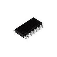
... Package Diagrams Document Number: 001-54707 Rev. *F Figure 14. 44-Pin TSOP II (51-85087) CY14B256LA 51-85087 *C Page [+] Feedback ...
Page 18
... Package Diagrams (continued) Document Number: 001-54707 Rev. *F Figure 15. 48-Pin SSOP (51-85061) CY14B256LA 51-85061 *D Page [+] Feedback ...
Page 19
... Package Diagrams (continued) Document Number: 001-54707 Rev. *F Figure 16. 32-Pin SOIC (51-85127) CY14B256LA 51-85127 *B 51-85127 *B Page [+] Feedback ...
Page 20
... Document Number: 001-54707 Rev. *F Document Conventions Units of Measure Symbol Unit of Measure °C degrees Celsius Hz Hertz kbit 1024 bits kHz kilohertz KΩ kilo ohms μA microamperes mA milliampere μF microfarads MHz megahertz μs microseconds ms millisecond ns nanoseconds pF picofarads V volts Ω ohms W watts CY14B256LA Page [+] Feedback ...
Page 21
... Document History Page Document Title: CY14B256LA 256-Kbit (32 K × 8) nvSRAM Document Number: 001-54707 Orig. of Submission Rev. ECN No. Change Date ** 2746918 GVCH/AESA 07/31/2009 *A 2772059 GVCH/PYRS 09/30/2009 *B 2829117 GVCH 12/16/09 *C 2894560 GVCH 03/18/10 *D 2995066 GVCH 07/28/2010 *E 3074570 GVCH 10/29/10 *F 3143330 GVCH 01/17/2011 Document Number: 001-54707 Rev. *F ...
Page 22
... Cypress against all charges. Use may be limited by and subject to the applicable Cypress software license agreement. Document Number: 001-54707 Rev. *F All products and company names mentioned in this document may be the trademarks of their respective holders. cypress.com/go/plc Revised January 20, 2011 CY14B256LA PSoC Solutions psoc.cypress.com/solutions PSoC 1 | PSoC 3 ...