CY7C1018DV33-10VXI Cypress Semiconductor Corp, CY7C1018DV33-10VXI Datasheet
CY7C1018DV33-10VXI
Specifications of CY7C1018DV33-10VXI
CY7C1018DV33-10VXI
Available stocks


Related parts for CY7C1018DV33-10VXI

CY7C1018DV33-10VXI Summary of contents
Page 1
... I/O pins. The eight input/output pins (I/O high-impedance state when the device is deselected (CE HIGH), the outputs are disabled (OE HIGH), or during a write operation (CE LOW, and WE LOW). The CY7C1018DV33 is available in Pb-free 32-pin 300-Mil wide Molded SOJ. I/O 0 I/O 1 ...
Page 2
... V = Max., 100MHz mA, OUT 1/t MAX RC Max > > < MAX Max > V – 0.3V > V – 0.3V < 0.3V CY7C1018DV33 Unit [2] ................................ –0. 0.3V CC Ambient V Speed CC Temperature 3.3V 0.3V – + –10 (Industrial) Unit Min. Max. 2.4 V 0 –0.3 0.8 V A –1 +1 A –1 ...
Page 3
... Test Conditions Still Air, soldered × 4.5 inch, four-layer printed circuit board [4] 3.0V GND 30 pF* Rise Time: 1 V/ns High-Z characteristics: R 317 3.3V OUTPUT 351 (c) CY7C1018DV33 Max. Unit 400-Mil Unit Wide SOJ C/W 57.61 C/W 40.53 ALL INPUT PULSES 90% ...
Page 4
... The minimum Write cycle time for Write Cycle No. 3 (WE controlled, OE LOW) is the sum of t Document #: 38-05465 Rev. *E [5] –10 (Industrial) Min. 100 values until the first memory access can be performed less than less than t , and t HZCE LZCE HZOE LZOE HZWE and t HZWE CY7C1018DV33 Unit Max. less than t for any given device ...
Page 5
... CE > > V – 0. < 0. DATA RETENTION MODE 3.0V > CDR [13, 14 OHA DOE DATA VALID 50% > 50 s or stable at V > 50 CC(min.) CC(min.) CY7C1018DV33 Min. Max. Unit 2 V – 0.3V 3. DATA VALID t HZOE t HZCE HIGH IMPEDANCE t PD ICC 50% ISB Page [+] Feedback ...
Page 6
... If CE goes HIGH simultaneously with WE going HIGH, the output remains in a high-impedance state. 18. During this period the I/Os are in the output state and input signals should not be applied. Document #: 38-05465 Rev SCE SA t SCE PWE t SD DATA VALID [16, 17 SCE PWE t SD DATA VALID IN CY7C1018DV33 Page [+] Feedback ...
Page 7
... I/O –I High Data Out Data High-Z Ordering Information Speed Ordering Code (ns) 10 CY7C1018DV33-10VXI Ordering Code Definitions 018 D V33 - 10 VX Please contact your local Cypress sales representative for availability of these parts. Document #: 38-05465 Rev. *E [11, 17 SCE PWE t SD DATA VALID Mode ...
Page 8
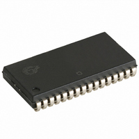
... Package Diagram Figure 1. 32-pin (300-Mil) Molded SOJ (51-85041) All product and company names mentioned in this document are the trademarks of their respective holders. Document #: 38-05465 Rev. *E CY7C1018DV33 51-85041 *B Page [+] Feedback ...
Page 9
... Document History Page Document Title: CY7C1018DV33, 1-Mbit (128K x 8) Static RAM Document Number: 38-05465 REV. ECN NO. Issue Date ** 201560 See ECN *A 238471 See ECN *B 262950 See ECN *C 307598 See ECN *D 520647 See ECN *E 3104943 12/08/2010 Document #: 38-05465 Rev. *E Orig. of Description of Change ...
Page 10
... The inclusion of Cypress products in life-support systems application implies that the manufacturer assumes all risk of such use and in doing so indemnifies Cypress against all charges. cypress.com/go/plc CY7C1018DV33 PSoC Solutions psoc.cypress.com/solutions ...