CY62256VNLL-70ZRXI Cypress Semiconductor Corp, CY62256VNLL-70ZRXI Datasheet - Page 2
CY62256VNLL-70ZRXI
Manufacturer Part Number
CY62256VNLL-70ZRXI
Description
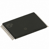
IC SRAM 256KBIT 70NS 28TSOP
Manufacturer
Cypress Semiconductor Corp
Type
Asynchronousr
Datasheet
1.CY62256VNLL-70SNXI.pdf
(13 pages)
Specifications of CY62256VNLL-70ZRXI
Memory Size
256K (32K x 8)
Package / Case
28-TSOP I
Format - Memory
RAM
Memory Type
SRAM
Speed
70ns
Interface
Parallel
Voltage - Supply
2.7 V ~ 3.6 V
Operating Temperature
-40°C ~ 85°C
Access Time
70 ns
Supply Voltage (max)
3.6 V
Supply Voltage (min)
2.7 V
Maximum Operating Current
30 mA
Maximum Operating Temperature
+ 85 C
Minimum Operating Temperature
- 40 C
Mounting Style
SMD/SMT
Number Of Ports
1
Operating Supply Voltage
3 V
Lead Free Status / RoHS Status
Lead free / RoHS Compliant
Lead Free Status / RoHS Status
Lead free / RoHS Compliant, Lead free / RoHS Compliant
Available stocks
Company
Part Number
Manufacturer
Quantity
Price
Company:

Part Number:
CY62256VNLL-70ZRXI
Manufacturer:
CYPRESS
Quantity:
1 292
Part Number:
CY62256VNLL-70ZRXI
Manufacturer:
CYPRESS/赛普拉斯
Quantity:
20 000


Product Portfolio
Pin Configurations
Pin Definitions
Document #: 001-06512 Rev. *B
CY62256VNLL
CY62256VNLL
CY62256VNLL
CY62256VNLL
1–10, 21, 23–26 Input
11–13, 15–19
27
20
22
14
28
Note
2. Typical values are included for reference only and are not guaranteed or tested. Typical values are measured at V
Pin Number
Product
GND
I/O 0
I/O 1
I/O 2
A 10
A 11
A 12
A 13
A 14
A 5
A 6
A 7
A 8
A 9
Narrow SOIC
13
14
1
2
3
4
5
6
7
8
9
10
11
12
Top View
Input/Output
Input/Control
Input/Control
Input/Control
Ground
Power Supply
28
27
26
25
24
23
22
21
20
19
18
17
16
15
Com’l
Automotive-A
Automotive-E
Ind’l
Type
I/O 3
V CC
WE
A 4
A 3
A 2
A 1
OE
A 0
CE
I/O 7
I/O 6
I/O 5
I/O 4
Range
V
WE
A
A
A
I/O
WE. When selected LOW, a WRITE is conducted. When selected HIGH, a READ is conducted
CE. When LOW, selects the chip. When HIGH, deselects the chip
OE. Output Enable. Controls the direction of the I/O pins. When LOW, the I/O pins behave as
outputs. When deasserted HIGH, I/O pins are tristated, and act as input data pins
GND. Ground for the device
V
OE
CC
A
A
A
A
A
A
A
A
A
10
11
CC
0
1
2
3
4
5
6
8
9
7
–A
0
–I/O
. Power supply for the device
14
22
23
24
25
26
27
28
1
2
3
4
5
6
7
. Address Inputs
Min
7
2.7
2.7
2.7
2.7
. Data lines. Used as input or output lines depending on operation
V
(not to scale)
CC
Top View
TSOP I
Range (V)
Typ
3.0
3.0
3.0
3.0
[2]
Max
3.6
3.6
3.6
3.6
21
20
19
18
17
16
15
14
13
12
11
10
9
8
A
CE
I/O
I/O
I/O
I/O
I/O
GND
I/O
I/O
I/O
A
A
A
0
14
13
12
7
6
5
4
3
2
1
0
Description
Operating, I
Typ
11
11
11
11
[2]
V
A
A
WE
OE
A
A
A
A
CC
A
A
A
A
A
11
10
9
8
7
6
5
4
3
2
1
26
25
24
23
22
7
6
5
4
CC
3
2
1
28
27
CC
Power Dissipation
= V
Max
(mA)
30
30
30
30
CC
Reverse Pinout
(not to scale)
Typ, T
Top View
TSOP I
A
= 25°C, and t
Standby, I
Typ
0.1
0.1
0.1
0.1
CY62256VN
[2]
AA
10
11
12
13
14
15
16
17
18
19
20
21
SB2
8
9
Page 2 of 13
= 70 ns.
Max
130
A
A
A
I/O
I/O
I/O
GND
I/O
I/O
I/O
I/O
I/O
CE
A
(μA)
10
10
12
13
14
0
5
0
1
2
3
4
5
6
7
[+] Feedback
Related parts for CY62256VNLL-70ZRXI
Image
Part Number
Description
Manufacturer
Datasheet
Request
R

Part Number:
Description:
CY62256VNLL-70SNXIT
Manufacturer:
Cypress Semiconductor Corp
Datasheet:

Part Number:
Description:
CY62256VNLL-70ZXIT
Manufacturer:
Cypress Semiconductor Corp
Datasheet:
Part Number:
Description:
IC SRAM 256KBIT 70NS 28SOIC
Manufacturer:
Cypress Semiconductor Corp
Datasheet:
Part Number:
Description:
IC SRAM 256KBIT 70NS 28TSOP
Manufacturer:
Cypress Semiconductor Corp
Datasheet:
Part Number:
Description:
CY62256VNLL-70SNXE
Manufacturer:
Cypress Semiconductor Corp
Datasheet:
Part Number:
Description:
CY62256VNLL-70SNXET
Manufacturer:
Cypress Semiconductor Corp
Datasheet:
Part Number:
Description:
CY62256VNLL-70ZRXIT
Manufacturer:
Cypress Semiconductor Corp
Datasheet:
Part Number:
Description:
CY62256VNLL-70ZXCT
Manufacturer:
Cypress Semiconductor Corp
Datasheet:
Part Number:
Description:
CY62256VNLL-70ZXE
Manufacturer:
Cypress Semiconductor Corp
Datasheet:
Part Number:
Description:
CY62256VNLL-70ZXET
Manufacturer:
Cypress Semiconductor Corp
Datasheet:
Part Number:
Description:
IC SRAM 256KBIT 70NS 28TSOP
Manufacturer:
Cypress Semiconductor Corp
Datasheet:
Part Number:
Description:
IC SRAM 256KBIT 70NS 28TSOP
Manufacturer:
Cypress Semiconductor Corp
Datasheet:
Part Number:
Description:
IC SRAM 256KBIT 70NS 28TSOP
Manufacturer:
Cypress Semiconductor Corp
Datasheet:
Part Number:
Description:
IC SRAM 256KBIT 70NS 28SOIC
Manufacturer:
Cypress Semiconductor Corp
Datasheet:
Part Number:
Description:
IC SRAM 256KBIT 70NS 28SOIC
Manufacturer:
Cypress Semiconductor Corp
Datasheet: