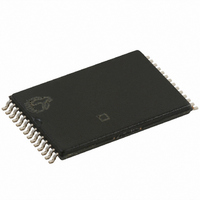
CY62256VNLL-70ZXI Cypress Semiconductor Corp, CY62256VNLL-70ZXI Datasheet

CY62256VNLL-70ZXI
Specifications of CY62256VNLL-70ZXI
CY62256VNLL-70ZXI
Available stocks
Related parts for CY62256VNLL-70ZXI
CY62256VNLL-70ZXI Summary of contents
Page 1
... Cypress Semiconductor Corporation Document Number: 001-06512 Rev. *E 256 K (32 K × 8) Static RAM Functional Description The CY62256VN family is composed of two high performance CMOS static RAM’s organized as 32K words by 8 bits. Easy memory expansion is provided by an active LOW chip enable (CE) and active LOW output enable (OE) and tristate drivers. ...
Page 2
Contents Product Portfolio .............................................................. 3 Pin Configurations ........................................................... 3 Pin Definitions .................................................................. 3 Maximum Ratings ............................................................. 4 Operating Range ............................................................... 4 Electrical Characteristics ................................................. 4 Capacitance ...................................................................... 5 Thermal Resistance .......................................................... 5 Data Retention Characteristics ....................................... 5 Switching Characteristics ................................................ ...
Page 3
... Product Portfolio Product Range CY62256VNLL Commercial CY62256VNLL Industrial CY62256VNLL Automotive-A CY62256VNLL Automotive-E Pin Configurations Narrow SOIC Top View I I/O 4 I/O 3 GND 15 14 Pin Definitions Pin Number Type 1–10, 21, 23–26 Input 11–13, 15–19 Input/Output 27 Input/Control 20 Input/Control 22 Input/Control ...
Page 4
Maximum Ratings Exceeding maximum ratings may shorten the useful life of the device. User guidelines are not tested. Storage temperature ................................ –65 °C to +150 °C Ambient temperature with power applied ........................................... –55 °C to +125 °C Supply voltage to ...
Page 5
Capacitance [5] Parameter Description C Input capacitance IN C Output capacitance OUT Thermal Resistance [5] Parameter Description θ Thermal resistance JA (junction to ambient) θ Thermal resistance JC (junction to case OUTPUT 50 pF INCLUDING JIG AND ...
Page 6
... HZWE 11. The internal write time of the memory is defined by the overlap of CE LOW and WE LOW. Both signals must be LOW to initiate a write and either signal can terminate a write by going HIGH. The data input set-up and hold timing should be referenced to the rising edge of the signal that terminates the write. ...
Page 7
... Address valid prior to or coincident with CE transition LOW. 16. The internal write time of the memory is defined by the overlap of CE LOW and WE LOW. Both signals must be LOW to initiate a write and either signal can terminate a write by going HIGH. The data input set-up and hold timing should be referenced to the rising edge of the signal that terminates the write. ...
Page 8
... Notes 20. The internal write time of the memory is defined by the overlap of CE LOW and WE LOW. Both signals must be LOW to initiate a write and either signal can terminate a write by going HIGH. The data input set-up and hold timing should be referenced to the rising edge of the signal that terminates the write. ...
Page 9
Typical DC and AC Characteristics NORMALIZED SUPPLY CURRENT vs. SUPPLY VOLTAGE 1.8 1.6 1.4 1.2 1.0 0 25°C 0.6 A 0.4 0.2 SUPPLY VOLTAGE (V) NORMALIZED ACCESS TIME vs. SUPPLY VOLTAGE 2.5 2.0 1 25°C A ...
Page 10
Typical DC and AC Characteristics TYPICAL ACCESS TIME CHANGE vs. OUTPUT LOADING 30.0 25 25° 20.0 15.0 10.0 5.0 0.0 0 200 400 CAPACITANCE (pF) Truth Table Inputs/Outputs H X ...
Page 11
... Ordering Information Speed Ordering Code (ns) 70 CY62256VNLL-70ZXC CY62256VNLL-70SNXI CY62256VNLL-70ZXI CY62256VNLL-70ZRXI CY62256VNLL-70SNXE CY62256VNLL-70ZXE Ordering Code Definitions CY 62 256 XXX Document Number: 001-06512 Rev. *E Package Package Type Diagram 51-85071 28-pin TSOP I (Pb-free) 51-85092 28-pin (300-mil) narrow SOIC (Pb-free) 51-85071 28-pin TSOP I (Pb-free) 51-85074 ...
Page 12
Package Diagrams Figure 8. 28-pin (300-mil) SNC (Narrow Body), 51-85092 Document Number: 001-06512 Rev. *E Figure 9. 28-pin TSOP 1 (8 × 13.4 mm), 51-85071 CY62256VN 51-85092 *C 51-85071 *I Page ...
Page 13
... Figure 10. 28-pin Reverse TSOP 1 (8 × 13.4 mm), 51-85074 Reference Information Acronyms Acronym Description CMOS complementary metal oxide semiconductor I/O input/output SRAM static random access memory VFBGA very fine ball grid array TSOP thin small outline package Document Number: 001-06512 Rev. *E Document Conventions Units of Measure Symbol Unit of Measure ° ...
Page 14
Document History Page Document Title: CY62256VN 256 K (32 K × 8) Static RAM Document Number: 001-06512 Orig. of Revision ECN Change ** 426504 NXR *A 488954 NXR *B 2769239 VKN/AESA *C 2901521 AJU *D 3119519 AJU *E 3329873 RAME ...
Page 15
... Cypress against all charges. Any Source Code (software and/or firmware) is owned by Cypress Semiconductor Corporation (Cypress) and is protected by and subject to worldwide patent protection (United States and foreign), United States copyright laws and international treaty provisions. Cypress hereby grants to licensee a personal, non-exclusive, non-transferable license to copy, use, modify, create derivative works of, and compile the Cypress Source Code and derivative works for the sole purpose of creating custom software and or firmware in support of licensee product to be used only in conjunction with a Cypress integrated circuit as specified in the applicable agreement ...


