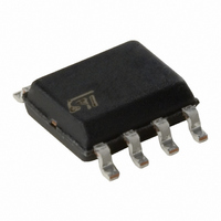
M95512-RMN6TP STMicroelectronics, M95512-RMN6TP Datasheet - Page 27

M95512-RMN6TP
Manufacturer Part Number
M95512-RMN6TP
Description
IC EEPROM 512KBIT 2MHZ 8SOIC
Manufacturer
STMicroelectronics
Specifications of M95512-RMN6TP
Format - Memory
EEPROMs - Serial
Memory Type
EEPROM
Memory Size
512K (64K x 8)
Speed
2MHz
Interface
SPI, 3-Wire Serial
Voltage - Supply
1.8 V ~ 5.5 V
Operating Temperature
-40°C ~ 85°C
Package / Case
8-SOIC (3.9mm Width)
Density
512Kb
Interface Type
Serial (SPI)
Organization
64Kx8
Access Time (max)
150ns
Frequency (max)
2MHz
Write Protection
Yes
Data Retention
40Year
Operating Supply Voltage (typ)
2.5/3.3/5V
Operating Temp Range
-40C to 85C
Supply Current
3mA
Operating Supply Voltage (min)
1.8V
Operating Supply Voltage (max)
5.5V
Operating Temperature Classification
Industrial
Mounting
Surface Mount
Pin Count
8
Lead Free Status / RoHS Status
Lead free / RoHS Compliant
Other names
497-6356-2
Available stocks
Company
Part Number
Manufacturer
Quantity
Price
Company:
Part Number:
M95512-RMN6TP
Manufacturer:
TDK
Quantity:
324
M95512-W, M95512-R, M95512-DR
6.9
Figure 16. Read Lock Status sequence
6.10
Read Lock Status (available only in M95512-DR devices)
The Read Lock Status instruction is used to read the lock status. To send this instruction to
the device, Chip Select (S) first has to be driven low. The bits of the instruction byte and
address bytes are then shifted in on Serial Data input (D). Address bit A10 must be 1, all
other address bits are Don't Care. The Lock bit is the LSB (least significant bit) of the byte
read on Serial Data output (Q). It is at ‘1’ when the lock is active and at ‘0’ when the lock is
not active. If Chip Select (S) continues to be driven low, the same data byte is shifted out.
The read cycle is terminated by driving Chip Select (S) high.
The instruction sequence is shown in
Lock ID (available only in M95512-DR devices)
The Lock ID instruction permanently locks the Identification Page in read-only mode. Before
this instruction can be accepted, a Write Enable (WREN) instruction must have been
executed. The Lock ID instruction is issued by driving Chip Select (S) low, sending the
instruction code, the address and a data byte on Serial Data input (D), and driving Chip
Select (S) high. In the address sent, A10 must be equal to 1, all other address bits are Don't
Care. The data byte sent must be equal to the binary value xxxx xx1x, where x = Don't Care.
Chip Select (S) must be driven high after the rising edge of Serial Clock (C) that latches in
the eighth bit of the data byte, and before the next rising edge of Serial Clock (C). Otherwise,
the Lock ID instruction is not executed.
Driving Chip Select (S) high at a byte boundary of the input data triggers the self-timed write
cycle whose duration is t
shown in
Figure
17.
W
(specified in
Doc ID 11124 Rev 12
Figure
Table 17
16.
and
Table
18). The instruction sequence is
Instructions
27/47


