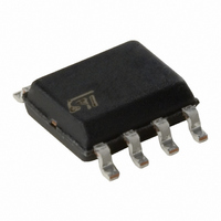
M24256-BRMN6TP STMicroelectronics, M24256-BRMN6TP Datasheet - Page 29

M24256-BRMN6TP
Manufacturer Part Number
M24256-BRMN6TP
Description
IC EEPROM 256KBIT 400KHZ 8SOIC
Manufacturer
STMicroelectronics
Specifications of M24256-BRMN6TP
Format - Memory
EEPROMs - Serial
Memory Type
EEPROM
Memory Size
256K (32K x 8)
Speed
400kHz
Interface
I²C, 2-Wire Serial
Voltage - Supply
1.8 V ~ 5.5 V
Operating Temperature
-40°C ~ 85°C
Package / Case
8-SOIC (3.9mm Width)
Organization
32 K x 8
Interface Type
I2C
Maximum Clock Frequency
0.4 MHz
Access Time
900 ns
Supply Voltage (max)
5.5 V
Supply Voltage (min)
1.8 V
Maximum Operating Current
0.5 mA
Maximum Operating Temperature
+ 85 C
Mounting Style
SMD/SMT
Minimum Operating Temperature
- 40 C
Operating Supply Voltage
2.5 V, 3.3 V, 5 V
Lead Free Status / RoHS Status
Lead free / RoHS Compliant
Other names
497-6348-2
Available stocks
Company
Part Number
Manufacturer
Quantity
Price
Part Number:
M24256-BRMN6TP
Manufacturer:
ST
Quantity:
20 000
M24256-BF, M24256-BR, M24256-BW, M24256-DR
Table 17.
1. Only new devices identified by the process letter K are qualified at 1 MHz (refer to TN0440 for more).
2. All values are referred to V
3. There is no min. or max. values for the input signal rise and fall times. It is however recommended by the
4. Characterized only, not tested in production.
5. With CL = 10 pF.
6. The I²C-bus specification does not define a min value of the data hold time (t
7. t
f
t
t
t
t
t
t
t
t
t
t
t
t
t
t
t
C
CHCL
CLCH
XH1XH2
XL1XL2
QL1QL2
DXCX
CLDX
CLQX
CLQV
CHDL
DLCL
CHDH
DHDL
W
NS
Symbol
I²C-bus specification that the input signal rise and fall times be less than 120 ns when f
t
falling edge SCL.
0.7V
(4)
CLQX
CLQV
(6)
(7)
CC
(4)
is the time (from the falling edge of SCL) required by the SDA bus line to reach either 0.3V
(Data out hold time) of the M24xxx devices offers a safe timing to bridge the undefined region of the
, assuming that R
1 MHz AC characteristics
f
t
t
t
t
t
t
t
t
t
t
t
t
t
t
SCL
HIGH
LOW
R
F
F
SU:DAT
HD:DAT
DH
AA
SU:STA
HD:STA
SU:STO
BUF
WR
Alt.
Clock frequency
Clock pulse width high
Clock pulse width low
Input signal rise time
Input signal fall time
SDA (out) fall time
Data in setup time
Data in hold time
Data out hold time
Clock low to next data valid (access time)
Start condition setup time
Start condition hold time
Stop condition setup time
Time between Stop condition and next
Start condition
Write time
Pulse width ignored (input filter on SCL and
SDA)
Test conditions specified in tables 7, 8,
bus
IL
(max) and V
× C
bus
Doc ID 6757 Rev 23
time constant is within the values specified in
IH
Parameter
(min).
(5)
(1)
9
and
Min.
HD;DAT
300
400
250
250
250
500
20
80
50
(3)
(3)
0
0
-
-
10
DC and AC parameters
(2)
Figure
). The min value of
C
Max.
6.
< 1 MHz.
120
500
50
(3)
(3)
1
5
-
-
-
-
-
-
-
-
-
(2)
CC
or
MHz
Unit
ms
ns
ns
ns
ns
ns
ns
ns
ns
ns
ns
ns
ns
ns
ns
29/42


