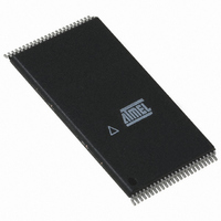
AT49F008AT-12TC Atmel, AT49F008AT-12TC Datasheet

AT49F008AT-12TC
Specifications of AT49F008AT-12TC
Available stocks
Related parts for AT49F008AT-12TC
AT49F008AT-12TC Summary of contents
Page 1
... The device contains a user-enabled “boot block” protection feature. Two versions of the feature are available: the AT49F008A/8192A locates the boot block at lowest order addresses (“bottom boot”); the AT49F008AT/8192AT locates it at highest order addresses (“top boot”). To allow for simple in-system reprogrammability, the AT49F008A(T)/8192A(T) does not require high-input voltages for programming. Reading data out of the device is similar to reading from an EPROM ...
Page 2
... The device is erased by executing the Erase command sequence; the device internally con- trols the erase operation. The memory is divided into four blocks for erase operations. There are two 4K word parameter block sections: the boot block, and the main memory array block. The typical number of program and erase cycles is in excess of 10,000 cycles. ...
Page 3
... Y DECODER INPUTS X DECODER DATA INPUTS/OUTPUTS V CC GND OE WE CONTROL LOGIC CE RESET Y DECODER INPUTS X DECODER AT49F008A(T)/8192A(T) AT49F008A AT49F008AT DATA INPUTS/OUTPUTS I/O0 - I/O7 I/O0 - I/O7 INPUT/OUTPUT INPUT/OUTPUT BUFFERS BUFFERS PROGRAM DATA PROGRAM DATA LATCHES LATCHES Y-GATING Y-GATING FFFFF MAIN MEMORY BOOT BLOCK ...
Page 4
... This feature does not have to be activated; the boot block’s usage as a write-protected region is optional to the user. The address range of the boot block is 00000H to 03FFFH for the AT49F008A; FC000H to FFFFFH for the AT49F008AT; 00000H to 01FFFH for the AT49F8192A; and 7E000H to 7FFFFH for the AT49F8192AT. ...
Page 5
... Software Product Identification Entry and Exit sections), a read from the following address location will show if programming the boot block is locked out – 00002H for the AT49F008A and AT49F8192A; FC002H for the AT49F008AT; and 7E002H for the AT49F8192AT. If the data on I/O0 is low, the boot block can be programmed; if the data on I/O0 is high, the program lockout feature has been enabled and the block cannot be pro- grammed ...
Page 6
... The ADDRESS FORMAT in each bus cycle is as follows: A15 - A0 (Hex); A-1 and A15 - A18 (Don’t Care). 2. The boot sector has the address range AT49F008AT; 00000H to 01FFFH for the AT49F8192A; and 7E000H to 7FFFFH for the AT49F8192AT 3. Either one of the Product ID Exit commands can be used. ...
Page 7
... X can Refer to AC programming waveforms. ± 12.0V 0.5V Manufacturer Code: 001FH Device Code: 22H (AT49F008A); 00A0H (AT49F8192A); 21H (AT49F008AT); 00A3H (AT49F8192AT). 5. See details under “Software Product Identification Entry/Exit” on page 13. DC Characteristics Symbol Parameter I Input Load Current LI I Output Leakage Current LO I ...
Page 8
AC Read Characteristics Symbol Parameter Address to t ACC Output Delay ( Output Delay CE ( Output Delay OE (3)( Output Float DF Output Hold from OE ...
Page 9
Input Test Waveforms and Measurement Level Output Test Load Pin Capacitance MHz ° C (1) Typ OUT Note: 1. This parameter is characterized and ...
Page 10
AC Word Load Characteristics Symbol Parameter Address, OE Setup Time AS OES t Address Hold Time AH t Chip Select Setup Time CS t Chip Select Hold Time CH t Write Pulse Width (WE or CE) WP ...
Page 11
Program Cycle Characteristics Symbol Parameter t Byte/Word Programming Time BP t Address Setup Time AS t Address Hold Time AH t Data Setup Time DS t Data Hold Time DH t Write Pulse Width WP t Write Pulse Width High ...
Page 12
Data Polling Characteristics Symbol Parameter t Data Hold Time Hold Time OEH ( Output Delay OE t Write Recovery Time WR Notes: 1. These parameters are characterized and not 100% tested. 2. See t ...
Page 13
... The device does not remain in identification mode if powered down. 4. The device returns to standard operation mode. 5. Manufacturer Code: 001FH Device Code: 22H (AT49F008A); 00A0H (AT49F8192A); 21H (AT49F008AT); 00A3H (AT49F8192AT) 6. Either one of the Product ID Exit commands can be used. 1199G–FLASH–11/02 (1) Boot Block Lockout Enable Algorithm (7) ...
Page 14
AT49F008A Ordering Information I (mA ACC Standby (ns) Active 0.3 AT49F8192A(T) Ordering Information I (mA ACC (ns) Active Standby 0.3 ...
Page 15
Packaging Information 44R – SOIC Dimensions in Millimeters and (Inches). Controlling dimension: Inches. 2325 Orchard Parkway San Jose, CA 95131 R 1199G–FLASH–11/02 0.508(0.020) 0.356(0.014) PIN 1 1.27(0.050) BSC 28.32(1.115) 28.07(1.105) 0.33(0.130) 1.27(0.050) 0º ~ 8º 1.00(0.039) 0.60(0.024) TITLE 44R, 44-lead ...
Page 16
TSOP Pin 1 Identifier e E Notes: 1. This package conforms to JEDEC reference MO-142, Variation CD. 2. Dimensions D1 and E do not include mold protrusion. Allowable protrusion 0.15 mm per side and on ...
Page 17
TSOP Pin 1 Identifier e E Notes: 1. This package conforms to JEDEC reference MO-142, Variation DD. 2. Dimensions D1 and E do not include mold protrusion. Allowable protrusion 0.15 mm per side and on ...
Page 18
... No licenses to patents or other intellectual property of Atmel are granted by the Company in connection with the sale of Atmel products, expressly or by implication. Atmel’s products are not authorized for use as critical components in life support devices or systems. ...


