AT27LV020A-90VI Atmel, AT27LV020A-90VI Datasheet
AT27LV020A-90VI
Specifications of AT27LV020A-90VI


Related parts for AT27LV020A-90VI


AT27LV020A-90VI Summary of contents
Page 1
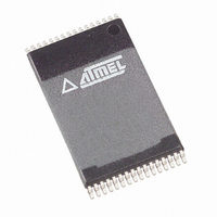
... At V accessed in less than 120 ns. With a typical power dissipation of only MHz and V = 3.3V, the AT27LV020A consumes less than one fifth the power of a stan- CC dard 5V EPROM. Standby mode supply current is typically less than 1 µA at 3.3V. The AT27LV020A is available in industry-standard JEDEC approved one-time pro- grammable (OTP) plastic PLCC, TSOP, and VSOP ...
Page 2
... Pin Configurations Pin Name A0 - A17 PGM NC 2.1 32-lead TSOP/VSOP (Type 1) Top View 2.2 32-lead PLCC – Top View AT27LV020A 2 Function Addresses Outputs Chip Enable Output Enable Program Strobe No Connect A11 A13 4 A14 5 A17 6 PGM 7 VCC 8 VPP 9 A16 10 A15 11 A12 A10 30 CE ...
Page 3
... Maximum Ratings” may cause permanent dam- age to the device. This is a stress rating only and functional operation of the device at these or any other conditions beyond those indicated in the (1) operational sections of this specification is not implied. Exposure to absolute maximum rating conditions for extended periods may affect device (1) reliability. (1) AT27LV020A 3 ...
Page 4
... Power Supply CC AT27LV020A 4 OE PGM Ai ( A17 = V ≤ 3.6V, or 4.5V ≤ ( Identification Code ≤ 5.5V 6.5V except A9 which is set to V and A0 which is toggled select the Device Code byte. IH AT27LV020A-12 -40° 85° C 3.0V to 3.6V 5V ± 10% Outputs D OUT High Z High OUT High Z 0549G–EPROM–12/07 ...
Page 5
... SB1 CC I (TTL 2 0.5V SB2 MHz mA OUT -400 µ and removed simultaneously with or after except during programming. The supply current would then be the sun AT27LV020A Min Max ±1 ± 0.5V 100 IL -0.6 0.8 2 0.4 2.4 ±1 ±5 10 100 ...
Page 6
... OE may be delayed This parameter is only sampled and is not 100% tested. 5. Output float is defined as the point when data is no longer driven. AT27LV020A after the falling edge of CE without impact after the address is valid without impact on t ACC OE AT27LV020A-12 Condition Min Max 120 120 ...
Page 7
... R F 12. Output Test Load Note: 13. Pin Capacitance ( MHz 25° C Symbol Typ OUT Note: 1. Typical values for nominal supply voltage. This parameter is only sampled and is not 100% tested. 0549G–EPROM–12/ including jig capacitance. Max 8 12 AT27LV020A Units Conditions OUT 7 ...
Page 8
... Programming Waveforms Notes: 1. The Input Timing Reference is 0.8V for and t are characteristics of the device but must be accommodated by the programmer. OE DFP 3. When programming the AT27LV020A a 0.1 µF capacitor is required across V transients. AT27LV020A 8 (1) and 2.0V for and ground to suppress spurious voltage PP 0549G–EPROM–12/07 ...
Page 9
... Program Pulse width tolerance is 100 µsec ± 5%. 17. Atmel’s AT27LV020A Integrated Product Identification Code Codes A0 Manufacturer 0 Device Type 1 Note: 1. The AT27LV020A has the same Product Identification Code as the AT27C020. Both are programming compatible. 0549G–EPROM–12/07 = 13.0 ± 0.25V PP Test Conditions ...
Page 10
... After the byte verifies properly, the next address is selected until all have been checked. V read again and compared with the original data to determine if the device passes or fails. AT27LV020A 10 is raised to 13.0V. Each address is first programmed with one 100 µ then lowered to 5 ...
Page 11
... Plastic Thin Small Outline Package (TSOP) 32V 32-Lead, Plastic Thin Small Outline Package (VSOP) 0549G–EPROM–12/07 Ordering Code AT27LV020A-12JI AT27LV020A-12TI AT27LV020A-12VI Ordering Code AT27LV020A-12JU AT27LV020A-12TU AT27LV020A-12VU Package Type AT27LV020A Package Operation Range 32J Industrial 32T (-40° 85° C) (1) 32V ...
Page 12
... Allowable protrusion is .010"(0.254 mm) per side. Dimension D1 and E1 include mold mismatch and are measured at the extreme material condition at the upper or lower parting line. 3. Lead coplanarity is 0.004" (0.102 mm) maximum. 2325 Orchard Parkway San Jose, CA 95131 R AT27LV020A 12 1.14(0.045) X 45˚ PIN NO. 1 IDENTIFIER E1 E ...
Page 13
... Lead coplanarity is 0.10 mm maximum. 2325 Orchard Parkway San Jose, CA 95131 R 0549G–EPROM–12/07 PIN SEATING PLANE A1 TITLE 32T, 32-lead ( Package) Plastic Thin Small Outline Package, Type I (TSOP) AT27LV020A 0º ~ 8º GAGE PLANE COMMON DIMENSIONS (Unit of Measure = mm) SYMBOL MIN NOM MAX A – – ...
Page 14
... E Notes: 1. This package conforms to JEDEC reference MO-142, Variation BA. 2. Dimensions D1 and E do not include mold protrusion. Allowable protrusion 0.15 mm per side and 0.25 mm per side. 3. Lead coplanarity is 0.10 mm maximum. 2325 Orchard Parkway San Jose, CA 95131 R AT27LV020A 14 PIN SEATING PLANE A1 TITLE ...
Page 15
... Disclaimer: The information in this document is provided in connection with Atmel products. No license, express or implied, by estoppel or otherwise, to any intellectual property right is granted by this document or in connection with the sale of Atmel products. EXCEPT AS SET FORTH IN ATMEL’S TERMS AND CONDI- TIONS OF SALE LOCATED ON ATMEL’S WEB SITE, ATMEL ASSUMES NO LIABILITY WHATSOEVER AND DISCLAIMS ANY EXPRESS, IMPLIED OR STATUTORY WARRANTY RELATING TO ITS PRODUCTS INCLUDING, BUT NOT LIMITED TO, THE IMPLIED WARRANTY OF MERCHANTABILITY, FITNESS FOR A PARTICULAR PURPOSE, OR NON-INFRINGEMENT ...