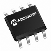
25AA080C-I/MS Microchip Technology, 25AA080C-I/MS Datasheet - Page 11

25AA080C-I/MS
Manufacturer Part Number
25AA080C-I/MS
Description
IC SRL EEPROM 1KX8 1.8V 8-MSOP
Manufacturer
Microchip Technology
Specifications of 25AA080C-I/MS
Memory Size
8K (1K x 8)
Package / Case
8-MSOP, Micro8™, 8-uMAX, 8-uSOP,
Format - Memory
EEPROMs - Serial
Memory Type
EEPROM
Speed
3MHZ, 5MHZ, 10MHZ
Interface
SPI, 3-Wire Serial
Voltage - Supply
1.8 V ~ 5.5 V
Operating Temperature
-40°C ~ 85°C
Organization
1 K x 8
Interface Type
SPI
Maximum Clock Frequency
10 MHz
Access Time
160 ns
Supply Voltage (max)
5.5 V
Supply Voltage (min)
1.8 V
Maximum Operating Current
5 mA
Maximum Operating Temperature
+ 85 C
Mounting Style
SMD/SMT
Minimum Operating Temperature
- 40 C
Operating Supply Voltage
2.5 V, 3.3 V, 5 V
Lead Free Status / RoHS Status
Lead free / RoHS Compliant
Lead Free Status / RoHS Status
Lead free / RoHS Compliant, Lead free / RoHS Compliant
Available stocks
Company
Part Number
Manufacturer
Quantity
Price
Company:
Part Number:
25AA080C-I/MS
Manufacturer:
MICROCHIP
Quantity:
12 000
3.6
The Write Status Register (WRSR) instruction allows the
user to select one of four levels of protection for the
array by writing to the appropriate bits in the Status reg-
ister. The array is divided up into four segments. The
user has the ability to write-protect none, one, two, or
all four of the segments of the array. The partitioning is
controlled as shown in Table 3-2.
The Write-Protect Enable (WPEN) bit is a nonvolatile
bit that is available as an enable bit for the WP pin. The
Write-Protect (WP) pin and the Write-Protect Enable
(WPEN) bit in the Status register control the program-
mable hardware write-protect feature. Hardware write
protection is enabled when WP pin is low and the
WPEN bit is high. Hardware write protection is disabled
when either the WP pin is high or the WPEN bit is low.
When the chip is hardware write-protected, only writes
to nonvolatile bits in the Status register are disabled.
See Table 3-3 for a matrix of functionality on the WPEN
bit.
See Figure 3-5 for the WRSR timing sequence.
FIGURE 3-7:
2004 Microchip Technology Inc.
SCK
CS
SO
SI
Write Status Register (WRSR)
0
0
0
WRITE STATUS REGISTER TIMING SEQUENCE
1
0
2
instruction
0
3
0
4
0
5
25AA080/25LC080/25C080
High-impedance
0
6
1
7
TABLE 3-2:
7
8
BP1
0
0
1
1
6
9
data to Status register
10
5
11
4
ARRAY PROTECTION
BP0
0
1
0
1
12
3
13
2
Array Addresses
Write-Protected
(0300h - 03FFh)
(0200h - 03FFh)
(0000h - 03FFh)
upper 1/4
14
upper 1/2
1
DS21230D-page 11
none
all
15
0


