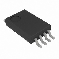
25LC040A-I/ST Microchip Technology, 25LC040A-I/ST Datasheet - Page 9

25LC040A-I/ST
Manufacturer Part Number
25LC040A-I/ST
Description
IC EEPROM 4KBIT 10MHZ 8TSSOP
Manufacturer
Microchip Technology
Specifications of 25LC040A-I/ST
Memory Size
4K (512 x 8)
Format - Memory
EEPROMs - Serial
Memory Type
EEPROM
Speed
10MHz
Interface
SPI, 3-Wire Serial
Voltage - Supply
2.5 V ~ 5.5 V
Operating Temperature
-40°C ~ 85°C
Package / Case
8-TSSOP
Memory Configuration
512 X 8 / 256 X 16
Ic Interface Type
SPI
Clock Frequency
10MHz
Supply Voltage Range
2.5V To 5.5V
Memory Case Style
TSSOP
No. Of Pins
8
Lead Free Status / RoHS Status
Lead free / RoHS Compliant
Available stocks
Company
Part Number
Manufacturer
Quantity
Price
Company:
Part Number:
25LC040A-I/ST
Manufacturer:
MCP
Quantity:
1 700
3.2
The device is selected by pulling CS low. The 8-bit
READ instruction is transmitted to the 25LCXXXA fol-
lowed by the 8-bit address. For the 25LC040A the MSb
(A8) is sent to the slave during the instruction
sequence. See Figure 3-1 for more details. After the
correct READ instruction and address are sent, the data
stored in the memory at the selected address is shifted
out on the SO pin. The data stored in the memory at the
next address can be read sequentially by continuing to
provide clock pulses. The internal Address Pointer is
automatically incremented to the next higher address
after each byte of data is shifted out. When the highest
address is reached, the address counter rolls over to
address 000h allowing the read cycle to be continued
indefinitely. The read operation is terminated by raising
the CS pin (Figure 3-1).
3.3
Prior to any attempt to write data to the 25LCXXXA, the
write enable latch must be set by issuing the WREN
instruction (Figure 3-4). This is done by setting CS low
and then clocking out the proper instruction into the
25LCXXXA. After all eight bits of the instruction are
transmitted, the CS must be brought high to set the
write enable latch. If the write operation is initiated
immediately after the WREN instruction without CS
being brought high, the data will not be written to the
array because the write enable latch will not have been
properly set.
Once the write enable latch is set, the user may
proceed by setting the CS low, issuing a WRITE instruc-
tion, followed by the 8-bit address, and then the data to
be written. Up to 16 bytes can be sent to the device
before a write cycle is necessary. The only restriction is
that all of the bytes must reside in the same page. Addi-
FIGURE 3-1:
© 2009 Microchip Technology Inc.
SCK
For the 24LC010A device both A8 and A7 are don’t cares.
For the 24LC020A device A8 is a don’t care.
CS
SO
SI
Read Sequence
Write Sequence
0
0
Instruction+Address MSb
1
0
0
2
READ SEQUENCE
3
0
A
4
8
5
0
High-impedance
6
1
1
7
A
8
7
A
9 10 11
Lower Address Byte
6
Preliminary
A
5
A
4
12 13 14 15 16 17 18 19 20 21 22 23
A
3
tionally a page address begins with ‘XXXX 0000’ and
ends with ‘XXXX 1111’. If the internal address counter
reaches ‘XXXX 1111’ and clock signals continue to be
applied to the ship, the address counter will roll back to
the first address of the page and over-write any data
that previously existed in those locations.
For the data to be actually written to the array, the CS
must be brought high after the Least Significant bit (D0)
of the n
brought high at any other time, the write operation will
not be completed. Refer to Figure 3-6 and Figure 3-4
for more detailed illustrations on the byte write
sequence and the page write sequence, respectively.
While the write is in progress, the STATUS register may
be read to check the status of the WIP, WEL, BP1 and
BP0 bits (Figure 3-6). A read attempt of a memory
array location will not be possible during a write cycle.
When the write cycle is completed, the write enable
latch is reset.
A
Note:
2
A
1
th
A
data byte has been clocked in. If CS is
0
Page write operations are limited to writing
bytes within a single physical page,
regardless of the number of bytes
actually being written. Physical page
boundaries start at addresses that are
integer multiples of the page buffer size (or
‘page size’) and, end at addresses that are
integer multiples of page size – 1. If a page
write command attempts to write across a
physical page boundary, the result is that
the data wraps around to the beginning of
the
previously stored there), instead of being
written to the next page as might be
expected. It is therefore necessary for the
application software to prevent page write
operations that would attempt to cross a
page boundary.
7
current
6
5
Data Out
25LCXXXA
4
page
3
2
(overwriting
DS22136B-page 9
1
0
data


