AT93C66A-10SU-2.7 Atmel, AT93C66A-10SU-2.7 Datasheet
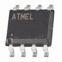
IC EEPROM 4KBIT 2MHZ 8SOIC

AT93C66A-10SU-2.7

Manufacturer Part Number
AT93C66A-10SU-2.7
Description
IC EEPROM 4KBIT 2MHZ 8SOIC
Manufacturer
Atmel

Specifications of AT93C66A-10SU-2.7

Format - Memory
EEPROMs - Serial
Memory Type
EEPROM
Memory Size
4K (512 x 8 or 256 x 16)
Speed
1MHz, 2MHz
Interface
3-Wire Serial
Voltage - Supply
2.7 V ~ 5.5 V
Operating Temperature
-40°C ~ 85°C
Package / Case
8-SOIC (3.9mm Width)
Organization
512 K x 8 or 256 K x 16
Interface Type
3-Wire
Maximum Clock Frequency
1 MHz
Supply Voltage (max)
5.5 V
Supply Voltage (min)
2.7 V
Maximum Operating Current
2 mA
Maximum Operating Temperature
+ 85 C
Mounting Style
SMD/SMT
Minimum Operating Temperature
- 40 C
Operating Supply Voltage
3.3 V, 5 V
Capacitance, Input
5 pF
Capacitance, Output
5 pF
Current, Input, Leakage
0.1 μA
Current, Operating
0.5 mA
Current, Output, Leakage
0.1
Data Retention
100 yrs.
Density
4K
Package Type
JEDEC SOIC
Temperature, Operating
-40 to +85 °C
Time, Address Setup
50
Time, Fall
250 ns
Time, Rise
250 ns
Voltage, Input, High
3.7 to 6.5 V
Voltage, Input, Low
0.8 V
Voltage, Output, High
2.4 V
Voltage, Output, Low
0.4 V
Voltage, Supply
2.7 to 5.5 V
Lead Free Status / RoHS Status
Lead free / RoHS Compliant

Available stocks

Company
Part Number
Manufacturer
Quantity
Price
Part Number:
AT93C66A-10SU-2.7
Manufacturer:
P-DUKE
Quantity:
2 000
Part Number:
AT93C66A-10SU-2.7
Manufacturer:
ATMEL
Quantity:
178
Part Number:
AT93C66A-10SU-2.7
Manufacturer:
ST
0
Part Number:
AT93C66A-10SU-2.7
Manufacturer:
ATMEL/爱特梅尔
Quantity:
20 000
Part Number:
AT93C66A-10SU-2.7
Quantity:
2 000
1. Features
2. Description
The AT93C56A/66A provides 2048/4096 bits of serial electrically erasable program-
mable read-only memory (EEPROM) organized as 128/256 words of 16 bits each
(when the ORG pin is connected to VCC) and 256/512 words of 8 bits each (when the
ORG pin is tied to ground). The device is optimized for use in many industrial and
commercial applications where low-power and low-voltage operations are essential.
The AT93C56A/66A is available in space-saving 8-lead PDIP, 8-lead JEDEC SOIC, 8-
lead EIAJ SOIC,
Grid Array (ULA), 8-lead TSSOP, and 8-ball dBGA2 packages.
The AT93C56A/66A is enabled through the Chip Select pin (CS) and accessed via a
three-wire serial interface consisting of Data Input (DI), Data Output (DO), and Shift
Clock (SK). Upon receiving a read instruction at DI, the address is decoded and the
data is clocked out serially on the data output pin DO. The write cycle is completely
self-timed and no separate erase cycle is required before write. The write cycle is only
enabled when the part is in the Erase/Write Enable State. When CS is brought “high”
following the initiation of a write cycle, the DO pin outputs the Ready/Busy status of
the part.
The AT93C56A/66A is available in 2.7V to 5.5V and 1.8V to 5.5V versions.
Low-voltage and Standard-voltage Operation
User-selectable Internal Organization
Three-wire Serial Interface
Sequential Read Operation
2 MHz Clock Rate (5V)
Self-timed Write Cycle (10 ms Max)
High Reliability
Automotive Devices Available
8-lead JEDEC PDIP, 8-lead JEDEC SOIC, 8-lead EIAJ SOIC, 8-lead Ultra Thin mini-MAP
(MLP 2x3), 8-lead Ultra Lead Frame Land Grid Array (ULA), 8-lead TSSOP and 8-ball
dBGA2 Packages
– 2.7 (V
– 1.8 (V
– 2K: 256 x 8 or 128 x 16
– 4K: 512 x 8 or 256 x 16
– Endurance: 1 Million Write Cycles
– Data Retention: 100 Years
CC
CC
= 2.7V to 5.5V)
= 1.8V to 5.5V)
8-lead Ultra Thin mini-MAP (MLP 2x3)
, 8-lead Ultra Lead Frame Land
Three-wire
Serial
EEPROM
2K (256 x 8 or 128 x 16)
4K (512 x 8 or 256 x 16)
AT93C56A
AT93C66A

Related parts for AT93C66A-10SU-2.7

AT93C66A-10SU-2.7 Summary of contents

Page 1

... Erase/Write Enable State. When CS is brought “high” following the initiation of a write cycle, the DO pin outputs the Ready/Busy status of the part. The AT93C56A/66A is available in 2.7V to 5.5V and 1.8V to 5.5V versions. , 8-lead Ultra Lead Frame Land Three-wire Serial EEPROM 2K (256 128 x 16) 4K (512 256 x 16) AT93C56A AT93C66A ...

Page 2

Table 2-1. Pin Configurations Pin Name Function CS Chip Select SK Serial Data Clock DI Serial Data Input DO Serial Data Output GND Ground VCC Power Supply ORG Internal Organization NC No Connect 3. Absolute Maximum Ratings* Operating Temperature......................................−55°C to ...

Page 3

Table 3-1. Pin Capacitance Applicable over recommended operating range from T Symbol Test Conditions C Output Capacitance (DO) OUT C Input Capacitance (CS, SK, DI) IN Note: 1. This parameter is characterized and is not 100% tested. Table 3-2. ...

Page 4

Table 3-3. AC Characteristics Applicable over recommended operating range from TTL Gate and 100 pF (unless otherwise noted) Symbol Parameter SK Clock f SK Frequency t SK High Time SKH t SK Low Time SKL Minimum ...

Page 5

... AT93C66A Ordering Information Ordering Code (2) AT93C66A-10PU-2.7 (2) AT93C66A-10PU-1.8 (2) AT93C66A-10SU-2.7 (2) AT93C66A-10SU-1.8 (2) AT93C66AW-10SU-2.7 (2) AT93C66AW-10SU-1.8 (2) AT93C66A-10TU-2.7 (2) AT93C66A-10TU-1.8 (2) AT93C66AU3-10UU-1.8 (3) AT93C66AD3-10DH-1.8 (2) AT93C66AY1-10YU-1.8 (Not recommended for new design) (3) AT93C66AY6-10YH-1.8 (4) AT93C66A-W1.8-11 Notes: 1. For 2.7V devices used in the 4.5V to 5.5V range, please refer to performance values in the AC and DC characteristics table. 2. “U” designates Green package + RoHS compliant. ...

Page 6

JEDEC SOIC e Side View Note: These drawings are for general information only. Refer to JEDEC Drawing MS-012, Variation AA for proper dimensions, tolerances, datums, etc. 1150 E. Cheyenne Mtn. Blvd. Colorado Springs, CO 80906 R 8.3 ...

Related keywords