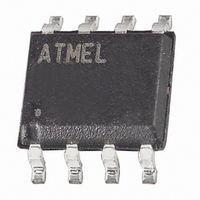
AT24C01BN-SH-B Atmel, AT24C01BN-SH-B Datasheet - Page 3

AT24C01BN-SH-B
Manufacturer Part Number
AT24C01BN-SH-B
Description
IC EEPROM 1KBIT 1MHZ 8SOIC
Manufacturer
Atmel
Specifications of AT24C01BN-SH-B
Format - Memory
EEPROMs - Serial
Memory Type
EEPROM
Memory Size
1K (128 x 8)
Speed
400kHz, 1MHz
Interface
I²C, 2-Wire Serial
Voltage - Supply
1.8 V ~ 5.5 V
Operating Temperature
-40°C ~ 85°C
Package / Case
8-SOIC (3.9mm Width)
Organization
128 K x 8
Interface Type
2-Wire
Maximum Clock Frequency
1 MHz
Access Time
550 ns
Supply Voltage (max)
5.5 V
Supply Voltage (min)
1.8 V
Maximum Operating Current
3 mA
Maximum Operating Temperature
+ 85 C
Mounting Style
SMD/SMT
Minimum Operating Temperature
- 40 C
Operating Supply Voltage
1.8 V, 5.5 V
Memory Configuration
128 X 8
Clock Frequency
1MHz
Supply Voltage Range
1.8V To 5.5V
Memory Case Style
SOIC
No. Of Pins
8
Rohs Compliant
Yes
Lead Free Status / RoHS Status
Lead free / RoHS Compliant
1. Pin Description
2. Memory Organization
5156E–SEEPR–10/08
SERIAL CLOCK (SCL): The SCL input is used to positive edge clock data into each EEPROM
device and negative edge clock data out of each device.
SERIAL DATA (SDA): The SDA pin is bidirectional for serial data transfer. This pin is open-
drain driven and may be wire-ORed with any number of other open-drain or open-collector
devices.
DEVICE/PAGE ADDRESSES (A2, A1, A0): The A2, A1 and A0 pins are device address inputs
that are hard wired for the AT24C01B. As many as eight 1K devices may be addressed on a sin-
gle bus system (device addressing is discussed in detail under the Device Addressing section).
WRITE PROTECT (WP): The AT24C01B has a write protect pin that provides hardware data
protection. The write protect pin allows normal read/write operations when connected to ground
(GND). When the write protect pin is connected to V
and operates as shown in
Table 1-1.
AT24C01B, 1K SERIAL EEPROM: Internally organized with 16 pages of 8 bytes each, the 1K
requires an 7-bit data word address for random word addressing. (See
WP Pin
Status
At V
At GND
CC
Write Protect
Full (1K) Array
Normal Read/Write Operations
Part of the Array Protected
24C01B
Table
1-1.
CC
, the write protection feature is enabled
Figure 8-2 on page
10)
3


