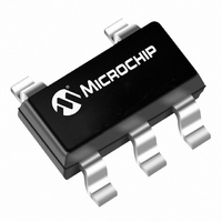
24AA16T-I/OT Microchip Technology, 24AA16T-I/OT Datasheet - Page 7

24AA16T-I/OT
Manufacturer Part Number
24AA16T-I/OT
Description
IC EEPROM 16KBIT 400KHZ SOT23-5
Manufacturer
Microchip Technology
Specifications of 24AA16T-I/OT
Memory Size
16K (2K x 8)
Package / Case
SOT-23-5, SC-74A, SOT-25
Operating Temperature
-40°C ~ 85°C
Format - Memory
EEPROMs - Serial
Memory Type
EEPROM
Speed
100kHz, 400kHz
Interface
I²C, 2-Wire Serial
Voltage - Supply
1.7 V ~ 5.5 V
Organization
8 Block x 256 x 8
Interface Type
I2C
Maximum Clock Frequency
0.4 MHz
Access Time
900 ns
Supply Voltage (max)
5.5 V
Supply Voltage (min)
1.7 V
Maximum Operating Current
5 mA
Maximum Operating Temperature
+ 85 C
Mounting Style
SMD/SMT
Minimum Operating Temperature
- 40 C
Operating Supply Voltage
1.8 V, 5.5 V
Lead Free Status / RoHS Status
Lead free / RoHS Compliant
Lead Free Status / RoHS Status
Lead free / RoHS Compliant, Lead free / RoHS Compliant
Other names
24AA16T-I/OT
24AA16TI/OT
24AA16TI/OT
Available stocks
Company
Part Number
Manufacturer
Quantity
Price
Company:
Part Number:
24AA16T-I/OT
Manufacturer:
MCP
Quantity:
15 000
Part Number:
24AA16T-I/OT
Manufacturer:
MICROCHIP/微芯
Quantity:
20 000
5.0
A control byte is the first byte received following the
Start condition from the master device (Figure 5-1).
The control byte consists of a four-bit control code.
For the 24XX16, this is set as ‘
and write operations. The next three bits of the control
byte are the block-select bits (B2, B1, B0). They are
used by the master device to select which of the eight
256 word-blocks of memory are to be accessed.
These bits are in effect the three Most Significant bits
(MSb) of the word address. It should be noted that the
protocol limits the size of the memory to eight blocks
of 256 words, therefore, the protocol can support only
one 24XX16 per system.
The last bit of the control byte defines the operation to
be performed. When set to ‘
selected. When set to ‘
Following the Start condition, the 24XX16 monitors the
SDA bus, checking the device type identifier being
transmitted and, upon receiving a ‘
slave device outputs an Acknowledge signal on the
SDA line. Depending on the state of the R/W bit, the
24XX16 will select a read or write operation.
FIGURE 5-2:
© 2009 Microchip Technology Inc.
DEVICE ADDRESSING
1
Control
Code
0
0
ADDRESS SEQUENCE BIT ASSIGNMENTS
’, a write operation is selected.
1
Control Byte
0
1
1010
’, a read operation is
B
2
Select
Block
1010
bits
’ binary for read
B
1
B
0 R/W
’ code, the
FIGURE 5-1:
A
7
Operation
Start Bit
Read
Write
•
S
Address Low Byte
24AA16/24LC16B
•
1
Control Code
•
0
Control
•
1010
1010
Code
Slave Address
1
•
CONTROL BYTE
ALLOCATION
0
•
A
0
B2 B1 B0 R/W ACK
Block Address
Block Address
Block Select
Select
Block
Bits
Acknowledge Bit
Read/Write Bit
DS21703J-page 7
R/W
1
0


