NLSV4T240MUTAG ON Semiconductor, NLSV4T240MUTAG Datasheet
NLSV4T240MUTAG
Specifications of NLSV4T240MUTAG
Available stocks


Related parts for NLSV4T240MUTAG

NLSV4T240MUTAG Summary of contents
Page 1
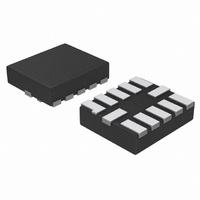
... Semiconductor Components Industries, LLC, 2007 July, 2007 - Rev. 0 ports are designed to track two and V respectively. Both CCB to the output B port Reached at GND V CCB B1 B2 NLSV4T240MUTAG B3 †For information on tape and reel specifications http://onsemi.com MARKING DIAGRAM 1 WBM G UQFN12 MU SUFFIX CASE 523AE WB = Specific Device Code M ...
Page 2
PIN ASSIGNMENT PIN FUNCTION V Input Port DC Power Supply CCA V Output Port DC Power Supply CCB GND Ground A Input Port n B Output Port n OE Output Enable MAXIMUM RATINGS Symbol Rating Supply ...
Page 3
DC ELECTRICAL CHARACTERISTICS Symbol Parameter V Input HIGH Voltage IH (An, OE) V Input LOW Voltage IL (An, OE) V Output HIGH Voltage OH V Output LOW Voltage OL I Input Leakage Current I I Power-Off Leakage Current OFF I ...
Page 4
TOTAL STATIC POWER CONSUMPTION (I 4.5 V (V) Min Max CCA 4.5 2 3.3 2 2.8 < 2 1.8 < 1 0.9 < 0.5 NOTE: Connect ground before applying supply voltage and V will not damage the ...
Page 5
Pulse Generator Figure 2. AC (Propagation Delay) Test Circuit Test PLH PHL PLZ PZL PHZ PZH equivalent (includes probe and jig capacitance ...
Page 6
... M NOTE 3 0.32 2.30 *For additional information on our Pb-Free strategy and soldering details, please download the ON Semiconductor Soldering and Mounting Techniques Reference Manual, SOLDERRM/D. N. American Technical Support: 800-282-9855 Toll Free USA/Canada Europe, Middle East and Africa Technical Support: Phone: 421 33 790 2910 Japan Customer Focus Center ...