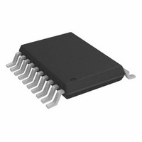
ADG3123BRUZ Analog Devices Inc, ADG3123BRUZ Datasheet - Page 10

ADG3123BRUZ
Manufacturer Part Number
ADG3123BRUZ
Description
IC XLATOR 8CH LOG-HV 20-TSSOP
Manufacturer
Analog Devices Inc
Datasheet
1.ADG3123BRUZ.pdf
(12 pages)
Specifications of ADG3123BRUZ
Logic Function
Translator
Number Of Bits
8
Input Type
CMOS
Output Type
Voltage
Number Of Channels
8
Number Of Outputs/channel
1
Differential - Input:output
No/No
Propagation Delay (max)
125ns
Voltage - Supply
2.3 V ~ 5.5 V
Operating Temperature
-40°C ~ 85°C
Package / Case
20-TSSOP
Supply Voltage
2.3 V ~ 5.5 V
No. Of Inputs
8
Propagation Delay
76ns
Logic Type
Level Translator
Supply Voltage Range
2.3V To 5.5V
Logic Case Style
TSSOP
No. Of Pins
20
Operating Temperature Range
-40°C To +85°C
Lead Free Status / RoHS Status
Lead free / RoHS Compliant
Data Rate
-
Lead Free Status / RoHS Status
Lead free / RoHS Compliant, Lead free / RoHS Compliant
Available stocks
Company
Part Number
Manufacturer
Quantity
Price
Company:
Part Number:
ADG3123BRUZ
Manufacturer:
Analog Devices Inc
Quantity:
1 970
Part Number:
ADG3123BRUZ
Manufacturer:
ADI/亚德诺
Quantity:
20 000
ADG3123
THEORY OF OPERATION
The ADG3123 is an 8-channel, noninverting CMOS to high
voltage level translator. Fabricated on an enhanced LC
process, the device is capable of operating at high supply
voltages while maintaining ultralow power consumption.
The device requires a dual-supply voltage, V
sets the low logic levels for all outputs and the high logic levels
for the Y7 and Y8 outputs. The V
The voltage applied to the V
level for the Y1 to Y6 outputs.
The device translates the CMOS logic levels applied to the A1 to
A8 inputs into high voltage bipolar levels available on the Y side
of the device at Pin Y1 to Pin Y8.
To ensure proper operation, V
or equal to V
Pin V
INPUT DRIVING REQUIREMENTS
The ADG3123 design ensures low input capacitance and
leakage current thereby reducing the loading of the circuit that
drives the input pins (Pin A1 to Pin A8) to a minimum. Its
input threshold levels are compliant with JEDEC standards for
drivers operated from supply voltages between 2.3 V and 5.5 V.
It is recommended that the inputs of any unused channel be
tied to a stable logic level (low or high).
OUTPUT LOAD REQUIREMENTS
The low output impedance of the ADG3123 allows each
channel to drive both resistive and capacitive loads. The
maximum load current is limited by the current carrying
capability of any given channel. If more channels are used, the
maximum load current per channel is reduced accordingly.
Note that the sum of the load currents on all channels should
never exceed the absolute maximum ratings specifications.
The average load current on each channel, I
determined using the formulas shown in the Capacitive Loads
and the Resistive Loads sections.
SS
should not exceed 35 V.
DDA
and the voltage between the Pin V
DDA
DDB
pin sets the output high logic
DDA
must always be greater than
pin acts as an analog input.
CHANNEL
DDB
and V
, can be
DDB
SS
2
and
MOS
, which
Rev. A | Page 10 of 12
Capacitive Loads
where:
F
C
V
V
outputs.
Resistive Loads
where:
D is the duty cycle of the input signal. D is defined as the ratio
between the high state duration of the signal and its period.
R
V
V
outputs.
POWER SUPPLIES
The ADG3123 operates from a dual-supply voltage. As good
design practice for all CMOS devices dictates, power up the
ADG3123 first (V
inputs (A1 to A8 and V
ADG3123, the voltage applied to the V
greater than or equal to V
Pin V
To ensure optimum performance, use decoupling capacitors on
all power supply pins. Furthermore, good engineering and
layout practice suggests placing these capacitors as close as
possible to the package supply pins.
O
L
L
SS
DDX
SS
DDX
is the load resistor in Ω.
is the frequency of the signal applied to the channel in Hz.
is the load capacitance in farads.
is the voltage applied to the V
is the voltage applied to the V
is V
is V
I
I
DDB
CHANNEL
CHANNEL
DDA
DDA
and Pin V
for Y1 to Y6 outputs, and V
for Y1 to Y6 outputs, and V
(
(
A
A
)
)
=
=
DDB
F
SS
D
O
should not exceed 35 V.
and V
×
×
V
DDA
C
DDX
DDA
L
). To ensure correct operation of the
SS
×
) before applying the signals to its
+
and the voltage between the
(
V
R
1 (
DDX
L
SS
SS
−
D
pin.
pin.
+
)
|
×
V
DDB
DDB
V
DDB
SS
SS
|)
pin must always be
for Y7 to Y8
for Y7 to Y8


