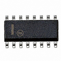
MC74ACT139DR2G ON Semiconductor, MC74ACT139DR2G Datasheet - Page 3

MC74ACT139DR2G
Manufacturer Part Number
MC74ACT139DR2G
Description
IC DECODER/DEMUX DUAL 1:4 16SOIC
Manufacturer
ON Semiconductor
Series
74ACTr
Type
Decoder/Demultiplexerr
Datasheet
1.MC74ACT139DTR2G.pdf
(11 pages)
Specifications of MC74ACT139DR2G
Circuit
1 x 2:4
Independent Circuits
2
Current - Output High, Low
24mA, 24mA
Voltage Supply Source
Single Supply
Voltage - Supply
4.5 V ~ 5.5 V
Operating Temperature
-40°C ~ 85°C
Mounting Type
Surface Mount
Package / Case
16-SOIC (3.9mm Width)
Logical Function
Decoder/Demux
Logic Family
ACT
Number Of Elements
2
Polarity
Inverting
Number Of Inputs
2
Number Of Outputs
4
Output Type
Open Drain
Propagation Delay Time
11ns
Package Type
SOIC
High Level Output Current
-24mA
Low Level Output Current
24mA
Operating Supply Voltage (typ)
5V
Operating Supply Voltage (max)
5.5V
Operating Supply Voltage (min)
4.5V
Operating Temp Range
-40C to 85C
Operating Temperature Classification
Industrial
Mounting
Surface Mount
Pin Count
16
Quiescent Current
8uA
Technology
CMOS
Lead Free Status / RoHS Status
Lead free / RoHS Compliant
Other names
MC74ACT139DR2G
MC74ACT139DR2GOSTR
MC74ACT139DR2GOSTR
Available stocks
Company
Part Number
Manufacturer
Quantity
Price
Company:
Part Number:
MC74ACT139DR2G
Manufacturer:
ON11
Quantity:
4 197
MAXIMUM RATINGS*
V
V
V
I
I
I
T
*Maximum Ratings are those values beyond which damage to the device may occur. Functional operation should be restricted to the Recom-
RECOMMENDED OPERATING CONDITIONS
V
V
t
t
T
T
I
I
1. V
2. V
IN
OUT
CC
r
r
OH
OL
, t
, t
stg
A
mended Operating Conditions.
J
CC
IN
OUT
CC
IN
Symbol
f
f
, V
Symbol
IN
IN
OUT
from 30% to 70% V
from 0.8 V to 2.0 V; see individual Data Sheets for devices that differ from the typical input rise and fall times.
Supply Voltage
DC Input Voltage, Output Voltage (Ref. to GND)
Input Rise and Fall Time (Note 1)
′AC Devices except Schmitt Inputs
Input Rise and Fall Time (Note 2)
′ACT Devices except Schmitt Inputs
Junction Temperature (PDIP)
Operating Ambient Temperature Range
Output Current − High
Output Current − Low
DC Supply Voltage (Referenced to GND)
DC Input Voltage (Referenced to GND)
DC Output Voltage (Referenced to GND)
DC Input Current, per Pin
DC Output Sink/Source Current, per Pin
DC V
Storage Temperature
CC
CC
or GND Current per Output Pin
; see individual Data Sheets for devices that differ from the typical input rise and fall times.
Parameter
Parameter
http://onsemi.com
3
V
V
V
V
V
CC
CC
CC
CC
CC
′ACT
′AC
@ 3.0 V
@ 4.5 V
@ 5.5 V
@ 4.5 V
@ 5.5 V
Min
−40
2.0
4.5
0
−
−
−
−
−
−
−
−
−0.5 to V
−0.5 to V
Typ
150
5.0
5.0
8.0
40
25
10
25
−
−
−
−
−0.5 to +7.0
−65 to +150
Value
±20
±50
±50
CC
CC
+0.5
+0.5
Max
V
140
−24
6.0
5.5
85
24
CC
−
−
−
−
−
Unit
Unit
ns/V
ns/V
mA
mA
mA
mA
mA
°C
°C
°C
V
V
V
V
V


