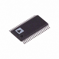
ADG3247BRU Analog Devices Inc, ADG3247BRU Datasheet - Page 10

ADG3247BRU
Manufacturer Part Number
ADG3247BRU
Description
IC SW BUS 2.5/3.3V 16BIT 38TSSOP
Manufacturer
Analog Devices Inc
Type
Bus Switchr
Datasheet
1.ADG3247BCPZ.pdf
(12 pages)
Specifications of ADG3247BRU
Rohs Status
RoHS non-compliant
Circuit
8 x 1:1
Independent Circuits
2
Voltage Supply Source
Single Supply
Voltage - Supply
2.5V, 3.3V
Mounting Type
Surface Mount
Package / Case
38-TSSOP
Operating Temperature
-
Current - Output High, Low
-
Available stocks
Company
Part Number
Manufacturer
Quantity
Price
Part Number:
ADG3247BRUZ
Manufacturer:
ADI/亚德诺
Quantity:
20 000
ADG3247
Bus Isolation
A common requirement of bus architectures is low capacitance
loading of the bus. Such systems require bus bridge devices that
extend the number of loads on the bus without exceeding the
specifications. Because the ADG3247 is designed specifically for
applications that do not need drive yet require simple logic func-
tions, it solves this requirement. The device isolates access to the
bus, thus minimizing capacitance loading.
Hot Plug and Hot Swap Isolation
The ADG3247 is suitable for hot swap and hot plug applications.
The output signal of the ADG3247 is limited to a voltage that is
below the V
fore the switch acts like a buffer to take the impact from hot
insertion, protecting vital and expensive chipsets from damage.
In hot-plug applications, the system cannot be shutdown when
new hardware is being added. To overcome this, a bus switch can
be positioned on the backplane between the bus devices and the
hot plug connectors. The bus switch is turned off during hot plug.
Figure 12 shows a typical example of this type of application.
Figure 10. 3.3 V to 1.8 V Voltage Translation, SEL = 0 V
Figure 11. Location of Bus Switched in a Bus
Isolation Application
BUS SWITCH
LOCATION
CC
supply, as shown in Figures 6, 8, and 10. There-
LOAD A
1.8V
V
0V
OUT
LOAD B
SWITCH
INPUT
LOAD C
3.3V SUPPLY
SEL = 0V
3.3V
LOAD D
V
IN
BACKPLANE
BUS/
–10–
There are many systems that require the ability to handle hot
swapping, such as docking stations, PCI boards for servers, and
line cards for telecommunications switches. If the bus can be
isolated prior to insertion or removal, then there is more control
over the hot swap event. This isolation can be achieved using a
bus switch. The bus switches are positioned on the hot swap card
between the connector and the devices. During hot swap, the
ground pin of the hot swap card must connect to the ground pin
of the back plane before any other signal or power pins.
Analog Switching
Bus switches can be used in many analog switching applications;
for example, video graphics. Bus switches can have lower on
resistance, smaller ON and OFF channel capacitance and thus
improved frequency performance than their analog counterparts.
The bus switch channel itself consisting solely of an NMOS
switch limits the operating voltage (see TPC 1 for a typical plot),
but in many cases, this does not present an issue.
High Impedance during Power-Up/Power-Down
To ensure the high impedance state during power-up or power-
down, BEx should be tied to V
the minimum value of the resistor is determined by the current-
sinking capability of the driver.
PACKAGE AND PINOUT
The ADG3247 is packaged in both a small 38-lead TSSOP or
a tiny 40-lead LFCSP package. The area of the TSSOP option
is 62.7 mm
This leads to a 43% savings in board space when using the LFCSP
package compared with the TSSOP package. This makes the
LFCSP option an excellent choice for space-constrained
applications.
The ADG3247 in the TSSOP package offers a flowthrough
pinout. The term flowthrough signifies that all the inputs are on
opposite sides from the outputs. A flowthrough pinout simplifies
the PCB layout.
Figure 12. ADG3247 in a Hot Plug Application
CPU
RAM
2
, while the area of the LFCSP option is 36 mm
CC
PLUG-IN
CARD (1)
PLUG-IN
CARD (2)
through a pull-up resistor;
CARD I/O
CARD I/O
REV. 0
2
.


