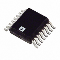
ADG3257BRQ-REEL Analog Devices Inc, ADG3257BRQ-REEL Datasheet - Page 4

ADG3257BRQ-REEL
Manufacturer Part Number
ADG3257BRQ-REEL
Description
IC MUX QUAD 3.3/5V HS 16-QSOP
Manufacturer
Analog Devices Inc
Type
Multiplexer/Demultiplexerr
Datasheet
1.ADG3257BRQZ-REEL.pdf
(12 pages)
Specifications of ADG3257BRQ-REEL
Rohs Status
RoHS non-compliant
Circuit
4 x 1:2
Independent Circuits
1
Voltage Supply Source
Single Supply
Voltage - Supply
3.3V, 5V
Operating Temperature
-40°C ~ 85°C
Mounting Type
Surface Mount
Package / Case
16-QSOP
Number Of Bits
8
Number Of Elements
1
Technology
CMOS
On Resistance
4Ohm
Propagation Delay Time
9ns
Package Type
QSOP
Operating Temp Range
-40C to 85C
Operating Temperature Classification
Industrial
Operating Supply Voltage (min)
3V
Operating Supply Voltage (typ)
3.3/5V
Operating Supply Voltage (max)
5.5V
Quiescent Current
1uA
Pin Count
16
Mounting
Surface Mount
Current - Output High, Low
-
Lead Free Status / Rohs Status
Not Compliant
ADG3257
V
Table 3.
Parameter
DC ELECTRICAL CHARACTERISTICS
CAPACITANCE
SWITCHING CHARACTERISTICS
DIGITAL SWITCH
POWER REQUIREMENTS
1
2
3
4
5
6
7
Temperature range is: Version B: −40°C to +85°C.
See Test Circuits section.
All typical values are at T
Guaranteed by design, not subject to production test.
The digital switch contributes no propagation delay other than the RC delay of the typical R
source. Because the time constant is much smaller than the rise/fall times of typical driving signals, it adds very little propagation delay to the system. Propagation
delay of the digital switch, when used in a system, is determined by the driving circuit on the driving side of the switch and its interaction with the load on the driven side.
Propagation delay matching between channels is calculated from on-resistance matching of worst-case channel combinations and load capacitance.
This current applies to the control pins only and represents the current required to switch internal capacitance at the specified frequency. The A and B ports contribute
no significant ac or dc currents as they transition.
CC
Input High Voltage
Input Low Voltage
Input Leakage Current
Off State Leakage Current
On State Leakage Current
Maximum Pass Voltage
A Port Off Capacitance
B Port Off Capacitance
A, B Port On Capacitance
Control Input Capacitance
Propagation Delay A to B or B to A, t
Propagation Delay Matching
Bus Enable Time BE to A or B
Bus Disable Time BE to A or B
Bus Select Time S to A or B
Maximum Data Rate
On Resistance
On-Resistance Matching
V
Quiescent Power Supply Current
Increase in I
CC
= 3.3 V ± 10%, GND = 0 V. All specifications T
Enable
Disable
1
4
CC
per Input
A
= 25°C, unless otherwise noted.
4
4, 7
4
6
PD
Symbol
V
V
I
I
I
V
C
C
C
C
t
t
t
t
t
R
ΔR
I
ΔI
I
OZ
OZ
CC
PHL
PZH
PHZ
SEL_EN
SEL_DIS
INH
INL
P
A
B
A
IN
ON
CC
, C
OFF
OFF
ON
, t
, t
, t
B
PLH
PZL
PLZ
ON
5
MIN
to T
Conditions
0 ≤ V
0 ≤ A, B ≤ V
0 ≤ A, B ≤ V
V
f = 1 MHz
f = 1 MHz
f = 1 MHz
f = 1 MHz
V
V
C
C
C
C
V
V
V
V
V
V
Digital inputs = 0 V or V
V
IN
A
A
A
A
A
A
A
A
CC
L
L
L
L
= 0 V, I
= 1 V, I
= 50 pF, R
= 50 pF, R
= 50 pF, R
= 50 pF, R
= 0 V, C
= 0 V, C
= 2 V p-p
= 0 V, I
= 1 V, I
= 0 V, I
= V
MAX
= 3.3 V, one input at 3.0 V; others at V
IN
Rev. E | Page 4 of 12
CC
, unless otherwise noted.
≤ 3.6 V
= 3.3 V, I
o
o
O
O
O
= 15 mA, 8 mA
= 15 mA, 8 mA
L
L
= 15 mA, 8 mA, T
= 15 mA, 8 mA, T
= 15 mA, 8 mA
CC
CC
= 50 pF
= 50 pF
2
L
L
L
L
= 500 Ω
= 500 Ω
= 500 Ω
= 500 Ω
O
= −5 μA
ON
of the switch and the load capacitance when driven by an ideal voltage
CC
A
A
= 25°C
= 25°C
CC
or GND
2.0
−0.3
2.3
1
1
3.0
Min
B Version
±0.01
±0.01
±0.01
2.6
7
5
11
4
0.01
5.5
4.5
8
6
933
2
4
0.2
0.001
Typ
3
+0.8
±1
±1
±1
2.8
0.10
0.04
9
8.5
12
9
4
5
7
8
5.5
1
200
Max
Unit
V
V
μA
μA
μA
V
pF
pF
pF
pF
ns
ns
ns
ns
ns
ns
Mbps
Ω
Ω
Ω
Ω
Ω
V
μA
μA


