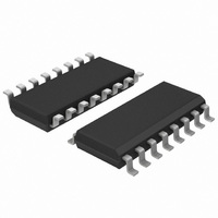
74LVC139D,118 NXP Semiconductors, 74LVC139D,118 Datasheet - Page 4

74LVC139D,118
Manufacturer Part Number
74LVC139D,118
Description
IC DUAL 2-4 DECODER/DEMUX 16SOIC
Manufacturer
NXP Semiconductors
Series
74LVCr
Type
Decoder/Demultiplexerr
Datasheet
1.74LVC139BQ115.pdf
(17 pages)
Specifications of 74LVC139D,118
Package / Case
16-SOIC (3.9mm Width)
Circuit
1 x 2:4
Independent Circuits
2
Current - Output High, Low
24mA, 24mA
Voltage Supply Source
Single Supply
Voltage - Supply
2.7 V ~ 3.6 V
Operating Temperature
-40°C ~ 125°C
Mounting Type
Surface Mount
Logic Family
LVC
Number Of Lines (input / Output)
2.0 / 4.0
Propagation Delay Time
50 ns
Supply Voltage (max)
3.6 V
Supply Voltage (min)
1.2 V
Maximum Operating Temperature
+ 125 C
Minimum Operating Temperature
- 40 C
Mounting Style
SMD/SMT
Number Of Input Lines
2.0
Number Of Output Lines
4.0
Logical Function
Decoder/Demux
Number Of Elements
2
Polarity
Inverting
Number Of Inputs
2
Number Of Outputs
4
Output Type
Standard
Package Type
SOIC W
High Level Output Current
-24mA
Low Level Output Current
24mA
Operating Supply Voltage (typ)
1.8/2.5/3.3V
Operating Supply Voltage (max)
3.6V
Operating Supply Voltage (min)
1.2V
Operating Temp Range
-40C to 125C
Operating Temperature Classification
Automotive
Mounting
Surface Mount
Pin Count
16
Technology
CMOS
Lead Free Status / RoHS Status
Lead free / RoHS Compliant
Lead Free Status / RoHS Status
Lead free / RoHS Compliant, Lead free / RoHS Compliant
Other names
74LVC139D-T
74LVC139D-T
935195990118
74LVC139D-T
935195990118
Philips Semiconductors
PINNING
2004 Mar 15
Dual 2-to-4 line decoder/demultiplexer
Fig.1 Pin configuration SO16 and (T)SSOP16.
PIN
10
11
12
13
14
15
16
1
2
3
4
5
6
7
8
9
GND
1A0
1A1
1Y0
1Y1
1Y2
1Y3
1E
1
2
3
4
5
6
7
8
1E
1A0
1A1
1Y0
1Y1
1Y2
1Y3
GND
2Y3
2Y2
2Y1
2Y0
2A1
2A0
2E
V
CC
SYMBOL
139
mna778
16
15
14
13
12
11
10
9
enable input (active LOW)
address input
address input
output (active LOW)
output (active LOW)
output (active LOW)
output (active LOW)
ground (0 V)
output (active LOW)
output (active LOW)
output (active LOW)
output (active LOW)
address input
address input
enable input (active LOW)
positive supply voltage
V
2E
2A0
2A1
2Y0
2Y1
2Y2
2Y3
CC
4
(1) The die substrate is attached to this pad using conductive die
attach material. It can not be used as a supply pin or input.
DESCRIPTION
Fig.2 Pin configuration DHVQFN16.
1A0
1A1
1Y0
1Y1
1Y2
1Y3
Top view
2
3
4
5
6
7
GND
1E
8
1
GND
V
(1)
2Y3
16
9
CC
Product specification
mna972
15
14
13
12
11
10
74LVC139
2E
2A0
2A1
2Y0
2Y1
2Y2


