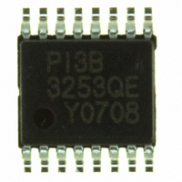
PI3B3253QE Pericom Semiconductor, PI3B3253QE Datasheet - Page 3

PI3B3253QE
Manufacturer Part Number
PI3B3253QE
Description
IC DUAL 4-1 BUS SW 16-QSOP
Manufacturer
Pericom Semiconductor
Type
Multiplexer/Demultiplexerr
Datasheet
1.PI3B3253QE.pdf
(5 pages)
Specifications of PI3B3253QE
Circuit
1 x 4:1
Independent Circuits
2
Voltage Supply Source
Single Supply
Voltage - Supply
3.3V
Operating Temperature
-40°C ~ 85°C
Mounting Type
Surface Mount
Package / Case
16-QSOP
Product
Multiplexer
Number Of Lines (input / Output)
8.0 / 2.0
Propagation Delay Time
0.25 ns at 3.3 V
Supply Voltage (max)
3.63 V
Supply Voltage (min)
2.97 V
Maximum Operating Temperature
+ 85 C
Minimum Operating Temperature
- 40 C
Mounting Style
SMD/SMT
Number Of Input Lines
8.0
Number Of Output Lines
2.0
Power Dissipation
0.5 W
Lead Free Status / RoHS Status
Lead free / RoHS Compliant
Current - Output High, Low
-
Lead Free Status / Rohs Status
Lead free / RoHS Compliant
Available stocks
Company
Part Number
Manufacturer
Quantity
Price
Company:
Part Number:
PI3B3253QE
Manufacturer:
Pericom
Quantity:
135
Part Number:
PI3B3253QE
Manufacturer:
PERICOM
Quantity:
20 000
Company:
Part Number:
PI3B3253QEX
Manufacturer:
PERICOM
Quantity:
11 943
Part Number:
PI3B3253QEX
Manufacturer:
DIODES/美台
Quantity:
20 000
Power Supply Characteristics
Notes:
1.
2.
3.
Switching Characteristics over Operating Range
Notes:
1.
2.
Applications Information
Logic Inputs
The logic control inputs can be driven up to +3.6V regardless of the supply voltage. For example, given a +3.3V supply, IN may be
driven low to 0V and high to 3.6V. Driving IN Rail-to-Rail
Power-Supply Sequencing and Hot Plug Information
Proper power-supply sequencing is recommended for all CMOS devices. Always apply V
input/output or control pins.
Rail-to-Rail is a registered trademark of Nippon Motorola, Ltd.
I
ΔI
t
t
t
t
t
IY
SY
PZH
PHZ
PLZ
CC
Parameters
CC
Parameters
For Max. or Min. conditions, use appropriate value specifi ed under Electrical Characteristics for the applicable device.
Typical values are at V
Per TTL driven input (control inputs only); I and Y pins do not contribute to I
This parameter is guaranteed but not tested on Propagation Delays.
The bus switch contributes no propagational delay other than the RC delay of the On-Resistance of the switch and the load capacitance. The
time constant for the switch alone is of the order of 0.25ns for 50pF load. Since this time constant is much smaller than the rise/fall times of
typical driving signals, it adds very little propagational delay to the system. Propagational delay of the bus switch when used in a system is
de ter mined by the driving circuit on the driving side of the switch and its interaction with the load on the driven side.
06-0332
Quiescent Power Supply Current
Supply Current per Input
@ TTL HIGH
Propagation Delay
Bus Select Time, Sn to Yn
Bus Enable Time, E to Yn
Bus Disable Time, En to Y
CC
= 3.3V, +25°C ambient.
De scrip tion
De scrip tion
(1,2)
In to Yn
V
V
CC
CC
®
Test Conditions
= Max.
= Max.
minimizes power consumption.
3
V
Test Conditions
V
IN
CC
IN
or V
R
C
= 3.0V
.
L
L
= GND
(1)
= 500Ω
= 50pF
CC
3.3V, Dual 4:1 Mux/DeMux NanoSwitch
(3)
Min.
CC
and GND before applying signals to
Min.
Typ.
1
1
1
0.1
(2)
Com.
Max.
Max.
750
0.25
3.0
4.0
3.8
5.2
PS8147J
PI3B3253
Units
Units
μA
ns
12/13/06
™


